Continue to Site

Welcome to EDAboard.com

Welcome to our site! EDAboard.com is an international Electronics Discussion Forum focused on EDA software, circuits, schematics, books, theory, papers, asic, pld, 8051, DSP, Network, RF, Analog Design, PCB, Service Manuals... and a whole lot more! To participate you need to register. Registration is free. Click here to register now.

How to implement "latch-up" guard rings and prevent parasitic lateral NPN at the same

Status
Not open for further replies.

mult

Junior Member level 1
Joined
Jan 17, 2013
Messages
18
Helped
0
Reputation
0
Reaction score
0
Trophy points
1,281
Activity points
1,442
How to implement "latch-up" guard rings and prevent parasitic lateral NPN at the same

Hi all.
I am trying to create latch-up guard rings for IO "low-side" BJT_36V and HVNMOS_36V according to TSMC BCD 0.18 design rule.
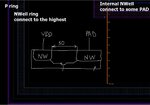
And there is a requirement of design rule to keep huge space between two Nwells connected to two different pads to prevent parasitic NPN. Space is so great (50um) that the very idea of creating rings seems impracticable.
Please see the picture.
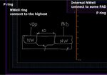
Image 7.jpg

If I use smaller distance I get DRC violations.

I don't know is it really possible to be turned on for this parasitic transistor in some the worst coincidence, so I am not sure if I can waive such DRC violations and use acceptable dimensions.

Please advice!
 

Attachments

  • Image 7.jpg
    Image 7.jpg
    125.4 KB · Views: 204

Re: How to implement "latch-up" guard rings and prevent parasitic lateral NPN at the

Space is so great (50um) that the very idea of creating rings seems impracticable.

If I use smaller distance I get DRC violations.

That's probably the min. distance between pads. What if you insert a p+ guardRing in between? Does the same design rule take effect? Can you find & show the text of the design rule responsible for this violation?
 

Re: How to implement "latch-up" guard rings and prevent parasitic lateral NPN at the

You can't "get rid of" parasitic BJTs in junction isolated
technologies. What you can do is (a) degrade the hFE
to where any SCR can't hold and (b) shunt the base to
that any SCR can't fire with any sane current injection
(this may be complemented by spec limitations on pin
currents, switch-node dV/dt, and so on - but these
had better be non-problematic to the user of the
device, their normal and abnormal conditions).

There ought to be detailed latchup design rules
and, you'd think, PCell switches (or rings built in,
that you don't get to mess with) in a well done
PDK.
 

Re: How to implement "latch-up" guard rings and prevent parasitic lateral NPN at the

What if you insert a p+ guardRing in between? Does the same design rule take effect? Can you find & show the text of the design rule responsible for this violation?
There is a special section in design rule called "Parasitic ESD Rule": "The Rule defines the minimum spacing between two n-type regions to prevent parasitic lateral npn from turning on and unexpected ESD failure"
Here is the basic rule:
"Minimum space between two HVNW connected to different potential PADs ...(conditions such as HV, presence of N buried layer, etc)... 50 um;
If the n-type regions are connected to PADs with same logic or power state, this violation can be waived."
Yes, even with using of p+ guard ring the same design rule take effect.
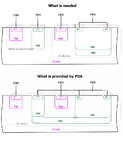
I explain the structure of rings in the picture.
Image 1.jpg


There ought to be detailed latchup design rules
and, you'd think, PCell switches (or rings built in,
that you don't get to mess with) in a well done
PDK.
You are right, there is a switch so-called "Sandwich Ring" in some of Pcells. But I think that is not exactly what is needed.
Please see the picture.
This switch adds N and P guard rings and extends NBL to the outer Nwell. Thus this N ring cannot be connected to potential other than PAD. But it doesn't make sence to connect N guard ring to not the most positive potential if the purpose is latch up prevention.
Image 2.jpg
 

Re: How to implement "latch-up" guard rings and prevent parasitic lateral NPN at the

If the n-type regions are connected to PADs with same logic or power state, this violation can be waived."

Is the VDD pad (always the left one in your pictures) used as a VDD supply pad, or is it just the connection of the n-well guard ring? In the latter case you could of course connect the 2 pads and waive the DRC violation.
 

Re: How to implement "latch-up" guard rings and prevent parasitic lateral NPN at the

Yes, "connected" ought to mean the supply pad makes
the rule work. However, if the cell is being verified at a
level lower than chip top level, maybe this pad is not
in the layout. In such a case maybe you need to add a
"frame" which has all supply pads (but as little else as
necessary) to validate the cell will not show errors once
embedded in its final home.

It might also be possible to spoof the rules by (say)
putting a 1x1um rectangle of M6Pad (or whatever -
parse the DRC rules backward to find what "connected"
means, to the rules set) on the supply lines.
 

Re: How to implement "latch-up" guard rings and prevent parasitic lateral NPN at the

Is the VDD pad (always the left one in your pictures) used as a VDD supply pad, or is it just the connection of the n-well guard ring? In the latter case you could of course connect the 2 pads and waive the DRC violation.

VDD is supply pad, and VDD is used to connect N Latchup ring as the highest voltage of the chip.
 

Re: How to implement "latch-up" guard rings and prevent parasitic lateral NPN at the

Space is so great (50um) that the very idea of creating rings seems impracticable.
Ok. Can't you connect the n-well guardRing directly to the IO-pad (the right one), and position the VDD-pad (used as power supply pad only) farer away?

It isn't necessary to use a higher n-well guardRing voltage than the (instantaneous) voltage of the pad which shall be protected.
 

Status
Not open for further replies.

Part and Inventory Search

Welcome to EDABoard.com

Sponsor

Back
Top