Welcome to our site! EDAboard.com is an international Electronics Discussion Forum focused on EDA software, circuits, schematics, books, theory, papers, asic, pld, 8051, DSP, Network, RF, Analog Design, PCB, Service Manuals... and a whole lot more! To participate you need to register. Registration is free. Click here to register now.
Could also be the channel current per W, for Vgs matching.
Although this suffers badly from delta-W effects and can't
really be counted on for more than a rough guide, against
unequal Ws.
It does not matter if the design is analog or not - current density is defined as current per unit width (for metals) or area or via (for vias).
If current I flows in a wire of width W, current density is: J=I/W.
The units are mA/um or A/um etc.
This is linear current density (current density per unit width of the wire, not area of the wire), assuming that current is uniformly distributed over the vertical cross-section of the wire (usually this is a very good approximation).
For vias, current density is J=I/A, where A is the area of via.
So this is current per unit area of the via.
To satisfy current density rules (for electromigration, or for ESD, or for latchup, etc.), simulation/verification tool checks simulated current density against some spec values and reports violations.
If you think of values in units of [mA/um] or [mA/via] for metal or polysilicon layers, you'll have to calculate such values from the process-dependent layer thicknesses.
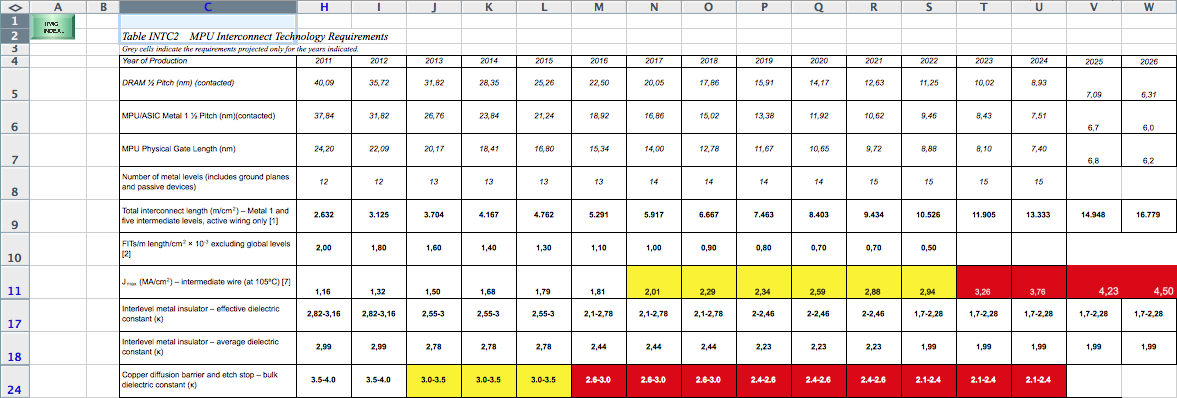
Metal wire current density is in the order of 10 MA/cm2 = 100mA/µm2 for electromigration limitation (s. p. 5 of the foll. PDF) : View attachment Electromigration_in_ICs.pdf
... and about a factor of 10 less for max. recommended current density in (intermediate) interconnect wires in highly integrated circuits (s. e.g. ITRS table 2011_INTC2, line 11) :
If you're talking digital you're likely to only care about
power busses, clock trees and I/Os.
Clock trees get a bonus from the periodically reversing
current flow. Unidirectional stuff like Vdd/Vss, and the
high or low legs of output buffers, can use time averaged
values.
Tungsten plug vias are a problem for aluminum interconnect
because they block material flow through the via (steady
state, aluminum will drift away from the "plug" and pile up
against the other side of it, leading to failure. There is also
an experimental-conduct issue relating to the tungsten
plug being a significant "heater" at high test current
densities, and local temps can be well above the forced
temperature that a lazy or ignorant reliability engineer
might use in the lifetime vs (J, T) calculations. If you are
struggling with rules that seem to require below 1E5 A/cm2
you might want to fight to get the derivations checked.
If you see a nice round number activation energy with
no independent physics-of failure backup, or you see a
interconnect temperature that matches the oven / chuck
temperature, you can say that the experiment was done
wrong. But good luck budging a foundry on that, it's not
only a bunch of extra work but an embarrassment as well.
There should be in a kit, a basic mA/um rule for each layer
and each via / contact. If you "own" the design then you
should put in the schematics and in a spreadsheet, the
worst case (P, V) current for any port that exceeds maybe
1/10 of this. A little book-keeping at the next levels up can
let you know when you start needing to pay attention and
use fatter than minimum metals, double up on vias, etc.
If you use native-material vias, you have to beware the
phenomenon of large beds filling the interior vias much less
uniformly than "lonely", doublet or quads (which can draw
from 360, 180 or 90 degrees of un-shared material during
sinter / reflow / hot dep) where interior vias share on all
sides, to the detriment of step coverage and fill uniformity.
But I suspect that "cmos layouts" may imply that this is
way more than you wanted to be told. Other than the
bit about keeping track as you build up from the bottom,
so you can spend time on this only when it becomes
appropriate.
Personally I like to go "way overkill" on bussing and
then I seldom run into EM driven relayout. Also helps
local power integrity in general. If you can afford the
area.
1. use foundry PDK and EM analysis tools (Voltus from Cadence, or RedHawk / Totem from Apache/ANSYS, or Silvaco tools, or Silicon Frontline tools, etc.) to simulate current flow corresponding to real operating conditions of the IC.
These tools will do the checking or current densities in every parasitic resistor and compare with the critical values, flagging the violations.
2. fix the layout to avoid EM violations.
An alternative is to do a manual checking - which is very hard for real designs unless they are very small and simple.
This site uses cookies to help personalise content, tailor your experience and to keep you logged in if you register.
By continuing to use this site, you are consenting to our use of cookies.