Continue to Site

Welcome to EDAboard.com

Welcome to our site! EDAboard.com is an international Electronics Discussion Forum focused on EDA software, circuits, schematics, books, theory, papers, asic, pld, 8051, DSP, Network, RF, Analog Design, PCB, Service Manuals... and a whole lot more! To participate you need to register. Registration is free. Click here to register now.

LDO Regulator & Forward Body Bias Technique

Status
Not open for further replies.

OmarMdDawi

Newbie level 3
Joined
May 5, 2017
Messages
3
Helped
0
Reputation
0
Reaction score
0
Trophy points
1
Activity points
32
Hi,
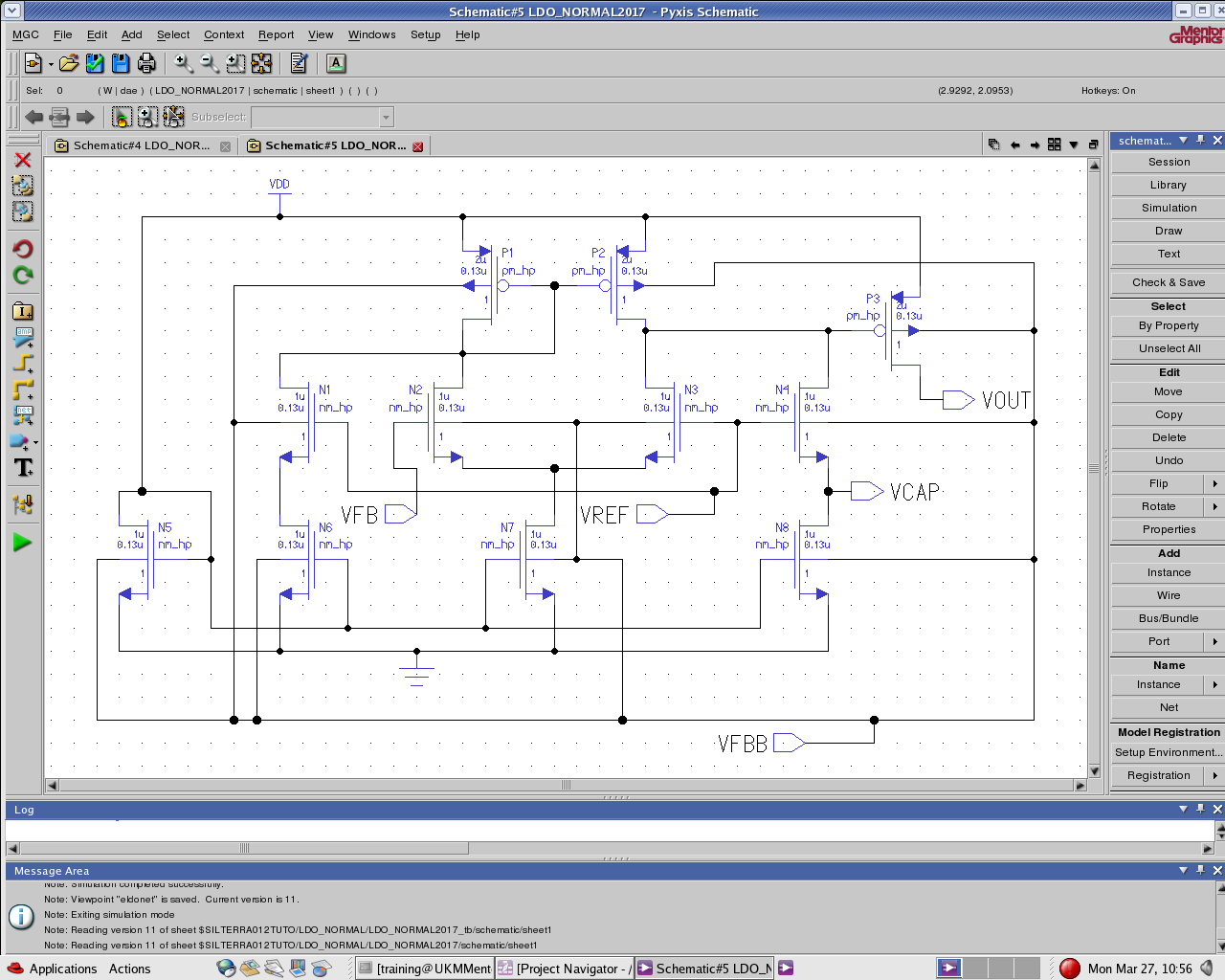
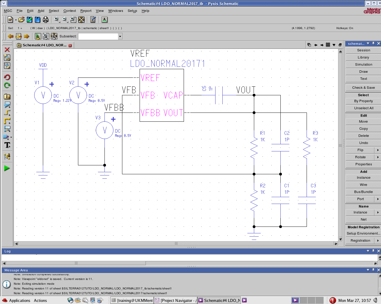
Can someone help me on LDO Regulator. FYI, i'm designing LDO Regulator with Forward Body Bias (FBB) technique using mentor graphic software (Silterra 0.13um). I had a problem where the power dissipation of this FBB LDO Regulator increased only 0.1mW compared to conventional circuit. Can someone explain this. Tq
 

Your problem description is not clear for me. What did you expect? Why - and for which transistor - do you need FBB in an LDO regulator? Show a schematic, please!
 

You can lower effective VT and maybe fix some headroom
problems, but for a PMOS pass transistor you would have
to drive or pump the body above the input rail. Then if you
have this ability, why not switch to a NMOS "ULDO" style?

Increasing power dissipation is generally not a good thing,
yet you seem to want more of it. Peculiar. Are you sure
you want the right things?
 

Thank you for your comments erikl...
Very sorry i forgot to attached the schematic diagram...really new here...
fyi sir, im applying FBB technique to all of the transistor NMOS & PMOS as per below schematic diagram...the aim is actually to achieved dropout voltage=100mV whereby the VDD=0.9V and Vout=0.8V...based on the parameter it is expected that by applying FBB technique the VDD voltage can be manipulated therefore the Power Dissipation would be reduce as compare to Conventional Circuit Without FBB (1.6683 mW). That is what im expected to achieved but Vice Vesa...is it possible for me to achieve that reducing in power dissipation?...Please help me sir...tq

FBB Schematic Diagram


Test Bench FBB Sample


TECHNOLOGY 0.13um (SILTERRA) – FBB BIAS
VDD @ VIN = 1.22 V
VOUT = 0.806 V
POWER DISSIPATION FBB = 2.0489 mW
POWER DISSIPATION CONVENTIONAL CIRCUIT = 1.6683 mW
VREF = 0.6 V
VFBB = 0.5 V
WIDTH NMOS = 1um
WIDTH PMOS = 2um
 

Thanks you Mr. dick_freebird for your comment...
actually im comparing the conventional circuit without FBB...with the circuit with FBB technique. Kindly please find the below schematic for your perusal sir...please help me sir tq very much

FBB Schematic Diagram


Test Bench FBB Circuit


TECHNOLOGY 0.13um (SILTERRA) – FBB BIAS
VDD @ VIN = 1.22 V
VOUT = 0.806 V
POWER DISSIPATION FBB TECHNIQUE = 2.0489 mW
POWER DISSIPATION WITHOUT FBB = 1.6886 mW
VREF = 0.6 V
VFBB = 0.5 V
WIDTH NMOS = 1um
WIDTH PMOS = 2um
 

... erikl...
...the aim is actually to achieved dropout voltage=100mV whereby the VDD=0.9V and Vout=0.8V
...based on the parameter it is expected that by applying FBB technique the VDD voltage can be manipulated therefore the Power Dissipation would be reduce as compare to Conventional Circuit Without FBB (1.6683 mW). That is what im expected to achieved but Vice Vesa...is it possible for me to achieve that reducing in power dissipation?

TECHNOLOGY 0.13um (SILTERRA) – FBB BIAS
VDD @ VIN = 1.22 V
VOUT = 0.806 V
POWER DISSIPATION FBB = 2.0489 mW
POWER DISSIPATION CONVENTIONAL CIRCUIT = 1.6683 mW
VREF = 0.6 V
VFBB = 0.5 V

Your VDD = 1.22V (equivalent to bandGap voltage?), which means the FBB for your PMOS transistors is -(VDD-VFBB) = -0.72V : way too high, probably enough to feed a lot of the PMOS transistors' source currents via the forward-biased channel-bulk junction (0.72V, silicon!) directly into the VFBB supply - with corresponding power consumption.

The method could work with a (probably for later planned) VDD=0.9V, but for your (now) VDD=1.22V you'd need 2 different VFBB sources, one for the NMOS, and one for the PMOS transistors.

Check & compare the source and drain currents of your PMOS transistors, and the sink current into the VFBB supply!
 

All FBB can do is lower the "effective VT". You are bound
by the junction forward voltage (and this gets smaller at
high temp) to maybe 0.4V. Body effect comes in at about
0.6V/V so maybe you lower VT by 0.2 - 0.25V. That's not
nothing, when you only have 0.9V (does this include, or
does it not, VDD tolerance?). But still this allows at most
maybe 0.7V "overdrive" of a FET which is naturally -0.4V
VT (all rough guesses here). And figure your error amp
gain will be in the tank when you get within a couple of
hundred mV of the VSS rail, so expect some issues with
accuracy and stability if you do operate there.

Still recommend you look at a NMOS pass device ULDO
if there's any expectation that a higher (like 2.5V) I/O
rail will be nearby as a general rule. But maybe the
projects has constraints besides the practical.

Dropout voltage (@load) may have to be achieved by
device width, once you decide on what gate drive
level (w/ or w/o FBB) can be used given the error amp
performance constraints. This then flows back into the
EA output drive current (costing you power there
instead (or additionally)).

Letting FBB turn on the parasitic BJT can make for all
kinds of nasty, like a pass FET (*PNP) that doesn't turn
off at low load currents, or has unexpected saturation
related behaviors (none of these being modeled in a
MOS SPICE compact model).

You might want FBB to be adaptive such that when you
are at low load / low |VGS| the body bias is zero (to
get minimum pass FET leakage) and when turning on
the pass FET hard, you also increase FBB. This is ala
"dynamic threshold" MOS biasing although you do not
want to drag the body as far as you do, the gate. It
might be simple to drive the body by a resistor divider
from the gate (thinking that at high output current,
a little body-bias-network loss is a nit, while at low,
you might spend less current in a passive divider than
a constant-power FBB bias amp).
 

Status
Not open for further replies.

Part and Inventory Search

Welcome to EDABoard.com

Sponsor

Back
Top