Continue to Site

Welcome to EDAboard.com

Welcome to our site! EDAboard.com is an international Electronics Discussion Forum focused on EDA software, circuits, schematics, books, theory, papers, asic, pld, 8051, DSP, Network, RF, Analog Design, PCB, Service Manuals... and a whole lot more! To participate you need to register. Registration is free. Click here to register now.

PMOS current source I-V characteristics

Status
Not open for further replies.

harian

Junior Member level 1
Joined
Jan 13, 2015
Messages
16
Helped
0
Reputation
0
Reaction score
0
Trophy points
1
Activity points
137
Hi Everybody,
i have a basic Pmos I-v Characteristics question. A PMos in cadence is connected as following(pls, see the below picture)..
Pmos.png
While simulating it, i got pmos diode like curve(pls see belwo)
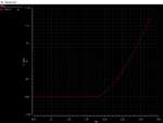
I-V.png
i m excepting a normal pmos I-v charistic like this (naturally inverted)
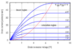
480px-IvsV_mosfet.svg.png.
can some one explaint he difference. I am simulation with cadence virtuoso.
 

I hope Vgs voltage is negative, right ??
 

What are the voltages at the gate and source?
You appear to have the MOSFET upside-down since you are applying the bias to the source and the drain is grounded.
 
Last edited:

I hope Vgs voltage is negative, right ??

ja the voltage is negative i.e. Vgs = Vg - Vdd and it is in my case -1.5,, I did also parametric simulation for Vgs -3.3 to 0 and Uds -3.3 to o.. the curve family are same.

- - - Updated - - -

What are the voltages at the gate and source?
You appear to have the MOSFET upside-down since you are applying the bias to the source and the drain is grounded.

the voltage are Vgs = -1.5 . i am thinking to use this PMOS as current source to fed a Nmos in simple common source amplifier, I wanted to just verify and learn. When i am doing the normal circuit with i.e not upside-down, then the curves are standard as in text books.
 

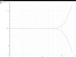
Simply because you plotted the source current instead of drain current. Ids is different of Isd ("just" a minus sign of difference).

take a look i did it for you:

https://obrazki.elektroda.pl/6513194300_1493825633.jpg


The red curve is Ids (what you wanna see) and the blue one is Isd (what you had plotted).

- - - Updated - - -

Simply because you plotted the source current instead of drain current. Ids is different of Isd ("just" a minus sign of difference).

take a look i did it for you:

blablabla.jpg

The red curve is Ids (what you wanna see) and the blue one is Isd (what you had plotted).
 

hi RS83, thx for reply,, I have seen ur plot. u r right that i have plotted the Isd instead of Ids. But still , the curve is far away from the nomal pmos curve. it is still like diode curve where the device start conducting 0.7 V.. There is no linear region, triode region and no saturation region at all.
regards
 

Correct your testbench first. Put source on the ground, connect drain to the voltage source. Fix gate voltage and sweep drain voltage.
 

hi RS83, thx for reply,, I have seen ur plot. u r right that i have plotted the Isd instead of Ids. But still , the curve is far away from the nomal pmos curve. it is still like diode curve where the device start conducting 0.7 V.. There is no linear region, triode region and no saturation region at all.
regards

My bad.

blablabla.jpg

Put your source at VDD (in mine it s 1.2V), then you connect your drain and your gate to different voltage source, then, you sweep the Vd voltage and plot the current Id.
 

And we have a diode carac plot because our first tests were with mos operating in reversed mode (you can check in the operating point).
 

My bad.

View attachment 138504

Put your source at VDD (in mine it s 1.2V), then you connect your drain and your gate to different voltage source, then, you sweep the Vd voltage and plot the current Id.

hi,, one question more,, did u mean , i need to connect one more voltage source to the drain,, in above case i have connected it to ground,, then vary vdd or the voltage source at the drain, can u pls upload ur testbench,, thx

- - - Updated - - -

what do u mean by mos in reversed mode,, can u pls expalin a little
 

Hi,

sdgfqsegfg.png

Put a positive Vg and simulate in DC within Vd varying from 0 to Vdd (here 1.2V).

The reversed mode is to put the wrong polarity in your MOS. Check about the breakdown Voltage of a MOS

gergqsrg.jpg


It s not really clear for me too, if someone else can explain us the physics besides this?
 

thx for the testbench
 

Don t forget like me to tie up your bulk to Vdd --'
 

Status
Not open for further replies.

Part and Inventory Search

Welcome to EDABoard.com

Sponsor

Back
Top