dzafar
Member level 4
Hello,
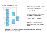
My question is regarding the image below.

Question: When we say read, does the image above show reading 1 bit. How I am seeing it is a WORD (8bits: A, B, C, D, E, F, G, H) comes in to 4 Muxes. Then 4 out of 8 bits get passed on to 4 Muxes and so on. And at the end the final MUX reads only 1 bit. But this does't make sense to me. Like why would you just read 1 bit? It would either me 1 or a 0. What use is that?
Could it be that A B C D E F G H are 8 WORDS instead of bits? What does the example "Example: a 256 bit x 8 bit memory would need 2040 logic blocks just to implement one read port!" at the end mean?
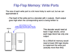
And then regarding Write Ports
Even though the image below is a good explanation but can someone use a bit simpler words to descibe the image below?

Thanks in advance
My question is regarding the image below.

Question: When we say read, does the image above show reading 1 bit. How I am seeing it is a WORD (8bits: A, B, C, D, E, F, G, H) comes in to 4 Muxes. Then 4 out of 8 bits get passed on to 4 Muxes and so on. And at the end the final MUX reads only 1 bit. But this does't make sense to me. Like why would you just read 1 bit? It would either me 1 or a 0. What use is that?
Could it be that A B C D E F G H are 8 WORDS instead of bits? What does the example "Example: a 256 bit x 8 bit memory would need 2040 logic blocks just to implement one read port!" at the end mean?
And then regarding Write Ports
Even though the image below is a good explanation but can someone use a bit simpler words to descibe the image below?

Thanks in advance