Continue to Site

Welcome to EDAboard.com

Welcome to our site! EDAboard.com is an international Electronics Discussion Forum focused on EDA software, circuits, schematics, books, theory, papers, asic, pld, 8051, DSP, Network, RF, Analog Design, PCB, Service Manuals... and a whole lot more! To participate you need to register. Registration is free. Click here to register now.

Please Help! SMPS efficiency only around 54%!

Status
Not open for further replies.

Electro-Boy

Newbie level 2
Joined
Apr 24, 2017
Messages
2
Helped
0
Reputation
0
Reaction score
0
Trophy points
1
Activity points
32
Hello,

I have a little problem.
I chose a project for school which I've managed to get working...
All the circuitry before and after the SMPS is working properly,
my only concern here is, that the SMPS is only working at an efficiency of around 54%.

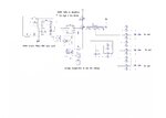
I've added my schematics for the SMPS part... feel free to use it even though its not good :)

I would apriciate any help or suggestions to bump the efficiency higher!

Ps. I can't feel any heat beeing generated... so where am I loosing all the power???
PPs. Sorry for my bad english, it's a bit rusty even though I'm 19...
 

Attachments

  • smpss.jpg
    smpss.jpg
    450.4 KB · Views: 110

Is there a link missing between the junction of D1/D2 and the top of C10/C11 ?

How are you measuring the efficiency? It will vary according to the load so we need to know the conditions yiou used to measure it.

Brian.
 

my only concern here is, that the SMPS is only working at an efficiency of around 54%...

Efficiency in this case is commonly defined as the (output power) *100/(input power). This is basically energy transfer ratio and (input power)-(output power) is simply wasted as heat. Most commonly this waste power appears around the seminconductor. If the transformer is made well, it wastes little power.

Usually the efficiency is not a constant but depends on the output power level (besides other factor). Because of switching delays the efficiency is usually lowest at the lowest output power.

During the design phase, you have selected some input voltage and efficiency also depends on the input voltage.

You will usually report the max efficiency your design can deliver. Hence put a resistive load close to the designed power.

Use an input voltage close to the design value. I expect you will get around 80% for this design. How you are measuring power?

If you want more professional looking results, make a graph of efficiency vs output power and efficiency vs input voltage.
 

Well I have measured the efficiency with 4 multimeters (fluke) i've tested them in school and they are prettey darn accurate!
one is for current input the other for voltage input and the same on the ouput... i had a load attached to get 3A current at 5 volts.

measurements:

all stable 5v out

7w in 4,5w out

20w in 10w out

46w in 17w out (~3.3A)

the interesting thing is that the efficiency decreases when im pushing more through the circuit... ?!?

another thing is that i get really bad spikes on the output... i'll atach a pic from the scope in an hour or so...

Betwixt, yea my bead there is a connection missing between the diodes and the caps... but its there on my breadboard...


c_mitra, I have wound the transformer pretty tightly and the primary is cut in half before and one after the secondaries to reduce eddy current...

i'll make the graph this afternoon

and i have to fix the spikes issue cause these galvanic isolated supplies are for lipo chargers... im a bit worried to give those nasty spikes to the linear chargers i've build...

Thanks for the replies :)
 

all stable 5v out

7w in 4,5w out

20w in 10w out

46w in 17w out (~3.3A)

There is some mistake in the circuit. You need to debug.

By the way, you need to also measure the phase to calculate the power. Just multiplying the voltage and current may not be optimal.

You also need to debug the spikes.
 

Hi,

For a DC output voltage:
P_out = I_avg x U_out.
No phase needed

The same is for input.

Klaus
 

For a DC output voltage:
P_out = I_avg x U_out.
No phase needed

The same is for input.

Thanks! I goofed up. I guess most modern multimeters will give you RMS current reading but the I(avg) and I(RMS) will be somewhat different. Right?
 

There are component Loss which has to be considered.

Conduction Loss (MOSFET & Diode) --> Conduction loss is generated in the RDS(ON) and the Vf of the Diode, (Loss Generates when that particular part turned on)

Switching Loss (Dynamic) --> There is particular time needed for transition between the parts on and off states. (So more power will be consumed during this transition period)

So Select MOSFET which is with value of low RDS(ON) and with fast switching transients,
Select Diodes with low Vf and fast recovery periods.

The switching loss also due to the capacitance, high value capacitances are tends to get charge slowly, which could cause the transition to be more and leads to consume more power, So CRSS & CGD in MOSFET data sheets should be verified and considered as these factors also leads to the efficiency issues which occurs during transition time.
 

46w in 17w out (~3.3A)

In this case, about 20W is being dissipated- quite a lot. Did you notice the MOSFETs or the transformer getting unreasonably hot?

The driver should stay reasonably cool.
 

Status
Not open for further replies.

Similar threads

Part and Inventory Search

Welcome to EDABoard.com

Sponsor

Back
Top