Continue to Site

Welcome to EDAboard.com

Welcome to our site! EDAboard.com is an international Electronics Discussion Forum focused on EDA software, circuits, schematics, books, theory, papers, asic, pld, 8051, DSP, Network, RF, Analog Design, PCB, Service Manuals... and a whole lot more! To participate you need to register. Registration is free. Click here to register now.

How can I improve my Clock/Calendar PIC board layout?

Status
Not open for further replies.

Garyl

Full Member level 5
Joined
Mar 28, 2017
Messages
253
Helped
6
Reputation
12
Reaction score
7
Trophy points
18
Activity points
2,633
Hey
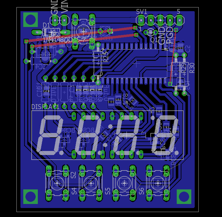
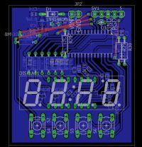
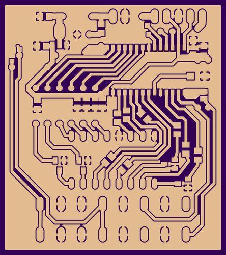
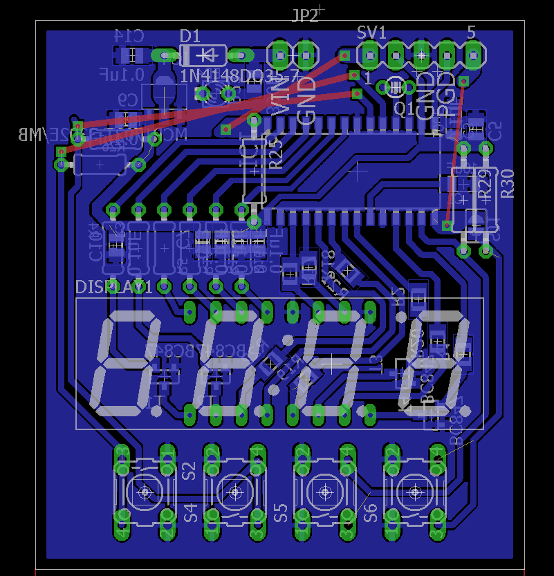
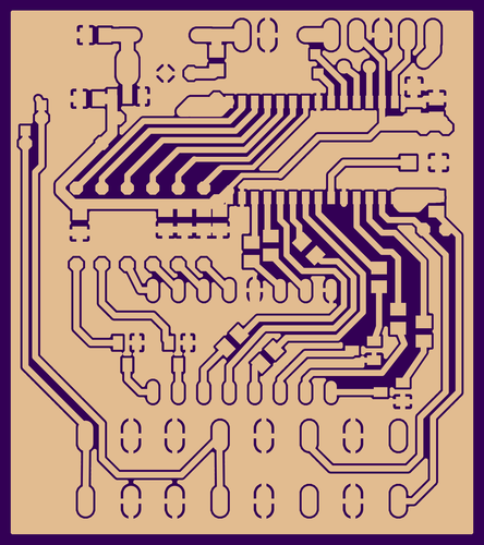
This is my 24F family clock/calendar with 7-segment display board:


It is using PIC INTERNAL OSCILLATOR and extra external oscillator for RTCC.
It has 4 digits 7-segmnent display, 3.3V LDO and 4 buttons and ICSP connector.

Can you tell me how can I improve my board layout and is the ground plane ok? Can I etch it already or is there something I can make better?
Thanks in advance!
 

Does the circuit have a backup battery or does it support one ? How does clock remember time after a power failure ?
 

Hi,

A homemade single layer layout.

Just from EMC view you should go for a double sided layout.

With this layout:
* I´d reduce the wire width from 0.6mm to 0.4mm or less.
* I´d increase the isolation to at least 0.25 mm
* route all air wires.
* use the DRC, but first set your DRC values.

It seems to be a LED display. It needs a lot of current. Thus the microcontroller may see varying supply voltage (caused by voltage drop). This may cause instability in clock frequency.

Check: doesn´t the XTAL need some capacitors?

I´m no friend of copper pour at all. And especially as GND. It pretends to be stable and reliable, but instead it causes additional inductance. Your GND loops may cause problems when HF sources like cellular phone, WIFI, Bluetooth is near your PCB. --> If possible make the TOP layer a solid GND plane without other traces.

I assume you don´t need to pass an EMC test. It is about impossible with this layout.

Klaus
 

How will it work ? The three red tracks (top layer) are crossing each other. Are they connected to each other in schematic ?
 

Thank you for replies! So, regarding your remarks:
- I usually solder those crystal capacitors in a bit tricky way, that why they are not in the Eagle
- I don't know how to make a good double-sided PCB at home so I make a single-sided one
- The top "tracks" are jumper wires in isolation, they are not connected
- There is no battery, there is only VIN/GND goldpin connector. I was planning to use just some old cellphone adapter that gives around 4V and keep the circuit plugged to it...

@KlausST - can you give more readings or something about that test? Is it in your opinion possible to do a good-enough single-sided layout for my circuit?

it's a first project so I'm trying to keep it simple, maybe the next version will include the CR battery.

I've modified the PCB:

now I am using a RESET button as a jumper
 

Hi,

double sided home made: I assume there are a lot of useful descriptions and even videos available.

For sure you need two films.
The tricky thing is how to align the top and the bottom foil.
I (some decades ago) used the TOP film to place two drills in the PCB (they should be far apart from each other. Maybe diagonally)
Then you could adjust both films to the drills.

The simplest though holes are at the THM connections. But you could use a piece of wire to create VIAs.

Klaus
 

double sided home made: I assume there are a lot of useful descriptions and even videos available.
How would I design that? top layer = vdd plane, bottom layer = gnd plane?

The simplest though holes are at the THM connections. But you could use a piece of wire to create VIAs.
What is THM? Through Hole M....?

Klaus, but my current PCB will work when etched and soldered correctly?
 

If the three top layer red tracks are jumpers then you should not get top layer printed on PCB. Then the jumper connections will be fine. Also top layer pads are optional.
 

Hi,

How would I design that? top layer = vdd plane, bottom layer = gnd plane?
Bottom layer as is, but without GND.
TOP layer GND
You need some adjustments.

Klaus, but my current PCB will work when etched and soldered correctly?
Most probably YES.
But don´t be surprised, if it fails when a cellular phone (or any other high frequency transmitter) is in close proximity to yur PCB.

What is THM? Through Hole M....?
It´s the opposite to SMD. What´s the "M" in SMD? I´m sure you will find out ;-)


Klaus
 

Isn't there any mounting hole for screws fastening ?
 

Status
Not open for further replies.

Part and Inventory Search

Welcome to EDABoard.com

Sponsor

Back
Top