Continue to Site

Welcome to EDAboard.com

Welcome to our site! EDAboard.com is an international Electronics Discussion Forum focused on EDA software, circuits, schematics, books, theory, papers, asic, pld, 8051, DSP, Network, RF, Analog Design, PCB, Service Manuals... and a whole lot more! To participate you need to register. Registration is free. Click here to register now.

i2c EEPROM 24AA128 PIC16F690 PIC C Compiler

Status
Not open for further replies.

JordanElektronika

Junior Member level 2
Joined
Jun 25, 2015
Messages
22
Helped
0
Reputation
0
Reaction score
0
Trophy points
1
Activity points
311
Good day! I am trying to write a code to "write to" and "read from" EEPROM 24AA128, but when I read, all I get is the control byte that I have sent. I know that i2c writes the data after the stop condition and before that it keeps it in a buffer, but still I see no reason why it does not work.

Schematic:
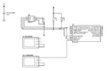
10. Intefraces-i2c-schematic.jpg

Source code:


Code C - [expand]
1
2
3
4
5
6
7
8
9
10
11
12
13
14
15
16
17
18
19
20
21
22
23
24
25
26
27
28
29
30
31
32
33
34
35
36
37
38
39
40
41
42
43
44
45
46
47
48
49
50
51
52
53
54
55
56
57
58
59
60
61
62
63
64
65
66
67
68
69
70
71
72
73
74
75
76
77
78
79
80
81
82
83
84
85
86
87
88
89
90
91
92
93
94
95
96
97
98
99
100
101
102
103
104
105
106
107
108
109
110
111
112
113
114
115
#include <16F690.h>
 
#define GP0 PIN_C0
#define GP1 PIN_C1
#define GP2 PIN_C2
#define GP3 PIN_C3
#define GP4 PIN_C4
#define GP5 PIN_C5
#define GP6 PIN_C6
#define GP7 PIN_C7
 
#fuses INTRC_IO, NOWDT, NOPROTECT, BROWNOUT                             /* Ext. oscilator, no watchdog, no code protect, no brownout (until voltage 
                                                                            rises on power up the PIC is held in reset = inactive) reset */
 
#use delay(clock=4M)                                                        /* Specify clock frequency, to use "delay_()" function */
#use rs232 (baud=9600, xmit=PIN_B7, rcv=PIN_B5, parity=N, bits=8, errors)
#use i2c (master, sda=PIN_B4, scl=PIN_B6, FAST, FORCE_HW)                                       /* Master mode, SDA pin = RB4, SCL pin = RB6, force hardware i2c functions */
 
#define SLAVE1_WRT_CON_BYTE 0b10100000                                      /* This byte should contain the control byte from the
                                                                            datasheet with control code, AN0, AN1, AN2 pins, READ or WRITE bit */
                                                                            /* bit<0> = 0 for write and 1 for read
                                                                            bits<1:3> = the values of the AN0:2 pins
                                                                            bits<4:7> = control code of "1010" for EEPROM24AA128 */
                                                                            /* !!! Dont forget that these must be put as the most significant bits first,
                                                                            A0, A1, A2 become A2, A1, A0, making:
                                                                            10100000 = control 4 bits/A2, A1, A0,/Read or write */
                                                                            /* HEX = 0xA0 */
                                                                            
#define SLAVE1_READ_CON_BYTE 0b10100001                                     /* This byte should contain the control byte from the
                                                                            datasheet with control code, AN0, AN1, AN2 pins, READ or WRITE bit */
                                                                            /* bit<0> = 0 for write and 1 for read
                                                                            bits<1:3> = the values of the AN0:2 pins
                                                                            bits<4:7> = control code of "1010" for EEPROM24AA128 */
                                                                            /* !!! Dont forget that these must be put as the most significant bits first,
                                                                            A0, A1, A2 become A2, A1, A0, making:
                                                                            10100001 = control 4 bits/A2, A1, A0,/Read or write */
                                                                            /* HEX = A1 */
                                                                            
#define SLAVE1_WRITE_ADDRESS_2_BYTES 0x00A2
#define SLAVE1_READ_ADDRESS_2_BYTES 0x00A3
//====================================
 
void main()
{
   unsigned int8 i;
   unsigned int8 data;
   
   while(1)
   {
      printf ("Starting i2c module....\r\n");
                            /* to write data */
      i2c_start();
      i2c_write(SLAVE1_WRT_CON_BYTE);           /* 1. Following the start condition, the next byte is control code (1010)\chip select (A2, A1, A0), R/W bit (logic low). 
                                                   This indicates to the addressed slave that the address high byte will follow after it has generated an Acknowledge bit */
      delay_ms (10);                            /* delay 10ms for the acknowledge bit to be sent, because we dont record it with the microcontroller */
      
      i2c_write (0x80);                     /* 2. The next byte is the high order byte of the word address and will be written into the Address Pointer of 24AA128 */
 
      i2c_write (0x00);                     /* 3. The next byte is the least significant address byte */     
      
      i2c_write (0x01);                     /* 4. After receiving another acknowledge signal from the 24AA128, the master will transmit tha data word to be written into 
                                                   the  addressed memory location */
                            /* After a byte write command, the internal address counter will point
                            /* to the address location following the one that was just written, because its automatically EEPROM hardware incremented */
      i2c_write (0x02);
      i2c_stop ();                  /* 5. After another acknowledge bit, the master sends the stop condition */
      delay_ms (10);                        /* The information is kept in a buffer, until the "stop condition", after which
                            /* it is recorded in the EEPROM, so we need a delay, after the "stop condition" */
 
      /* to write data */
      i2c_start();
      i2c_write(SLAVE1_WRT_CON_BYTE);           /* 1. Following the start condition, the next byte is control code (1010)\chip select (A2, A1, A0), R/W bit (logic low). This indicates to the addressed slave that the address high byte will follow after it has generated an Acknowledge bit */
      delay_ms (10);                    /* delay 10ms for the acknowledge bit to be sent, because we dont record it with the microcontroller */
      
      i2c_write (0x80);                 /* 2. The next byte is the high order byte of the word address and will be written into the Address Pointer of 24AA128 */
 
      i2c_write (0x00);                 /* 3. The next byte is the least significant address byte */     
      
      i2c_write (0x02);                 /* 4. After receiving another acknowledge signal from the 24AA128, the master will transmit tha data word to be written into the addressed memory location */
                            /* After a byte write command, the internal address counter will point
                            /* to the address location following the one that was just written, because its automatically EEPROM hardware incremented */
      i2c_write (0x02);
      i2c_stop ();                  /* 5. After another acknowledge bit, the master sends the stop condition */
      delay_ms (10);                        /* The information is kept in a buffer, until the "stop condition", after which
         
                            /* To read data from a random address */
      i2c_start();
      i2c_write(SLAVE1_WRT_CON_BYTE);           /* 1. Following the start condition, the next byte is control code (1010)\chip select (A2, A1, A0), R/W bit (logic low). 
                                                   This indicates to the addressed slave that the address high byte will follow after it has generated an "acknowledge bit".
                                                   We set "the internal address pointer" as a part of a "write" operation, in
                                                   order to be able to use "sequential read" */
     
      i2c_write (0x80);                 /* 2. The next byte is the high order byte of the word address and will be written into the Address Pointer of 24AA128 */
 
      i2c_write (0x00);                 /* 3. The next byte is the least significant address byte */
      
      i2c_start ();                     /* 4. We send a start condition, instead of a "stop condition", after the "internal address pointer" has been set in
                                  a "write" operation */
      
      i2c_write (SLAVE1_READ_CON_BYTE);         /* 5. For sequentual read, we send a "read" control byte, after the "internal address pointer" has
                                                   been set in a "write" operation and after that a "start condition" has been generated */
                               
      for (i=0; i<2 ;i++)
      {  
     data = i2c_read(0);
      
         output_c (data);
         delay_ms(1000);
      }
     i2c_stop ();                   /* 6. The data for the EEPROM is kept in a buffer, until the stop condition is issues,
                               and written after that, so we need a delay after the stop condition */
                            /* We make the delay 1 sec, in order to test the result of the program */
delay_ms (1000);
  }
}

 
Last edited by a moderator:

didn't see your code yet on common error would be wrong read address then write operation in most of the EEPROM i2c logic.

Rightly guess you are using READ: 0xa3
Write: 0xa2

but it should be as per your schematic READ: 0xa1
Write:0xa0
 
Last edited:

Your code is messy. Take I2C driver, google it if you can't write your own. Than the same way find how to work with I2C EEPROM. One of the most popular topics btw.
Write sequence:
1. Start
2. Send device address. If no ACK, stop and return error
3. Send memory address 8/16/32 bit depends of used eeprom
4. Send the data to write byte by byte in a row. Last one should be send without ACK.
5. Stop

Reading:
1. Start
2. Send device address. Return if no ACK followed by stop.
3. Send memory location address
4. Start again
5. Send device address+1 for reading
6. Read data byte by byte in a row
7. Stop

Simple!

To ud23: The code is in the dropbox link and so is the schematic.

To Easyrider83:
Why is it messy?
According to the datasheet of EEPROM 24AA128, the sequence is like this:
Write sequence:
1. Start condition.
*2. Send control byte with control code (1010), device address (A2, A1, A0), read/write bit (1/0), making 1 control byte of "10100000".
*3. Send device address high order byte (0x80 in this case), after an acknowledge send the low order byte (0x00 in this case).
4. After another acknowledge signal, send the data to write byte by byte in a row. Last one should be send without ACK.
5. Stop condition.

Reading:
1. Start
*2. Send control code (1010), EEPROM address (A2, A1, A0), read or write bit (0 or 1), making 1 whole control byte of "10100001".
3. After an acknowledge signal (the 9th bit) Send memory location address high byte order (0x80 in this case).
* After another acknowledge send memory location address low byte order (0x00 in this case).
*4. After another acknowledge send start condition again for random or sequential reading.
*5. The address is set as a part of the write operation (the first 4 steps, before we send another start condition terminating the write operation and starting a new read operation, however not before the internal address pointer was already set as a part of the write operation.
*6. Send the control byte for reading "10100001", after every operation the internal address pointer of EEPROM 24AA128 is automatically incremented by the EEPROM hardware inside.
7. Stop

Simple!

Is anyone familiar with this compiler? Has anyone done any communication with EEPROM 24XX128 and i2c and can you explain please?
 

This is my driver for 24xxx and 25xxx memories
**broken link removed**
It supports different page sizes and interfaces like I2C and SPI.
I suppose, it will be a bit compicated for you. But there is no mess.
 

Status
Not open for further replies.

Similar threads

Part and Inventory Search

Welcome to EDABoard.com

Sponsor

Back
Top