boylesg
Advanced Member level 4
- Joined
- Jul 15, 2012
- Messages
- 1,023
- Helped
- 5
- Reputation
- 10
- Reaction score
- 6
- Trophy points
- 1,318
- Location
- Epping, Victoria, Australia
- Activity points
- 11,697
Schematic:
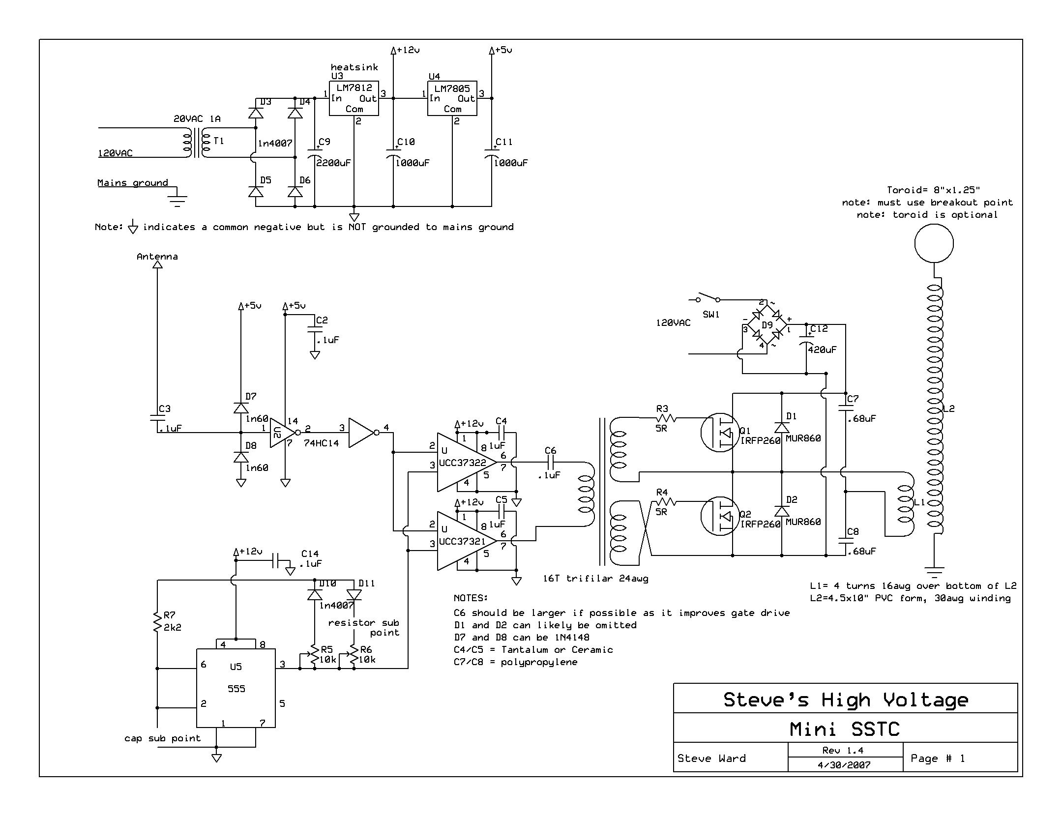
GDT: N30, 4 x AWG30 twisted tightly to form 3 wires, these were then twisted together to form a trifilar strand.

How would one apply an RC snubber to the above schematic. Increasing the value of R3 and R4 is suggested but if I increase the value too much then it will reduce the current into the FET gates significantly.
Ringing on GDT primary (scale 1uS)

Ringing on GDT secondaries (scale 1uS)


GDT: N30, 4 x AWG30 twisted tightly to form 3 wires, these were then twisted together to form a trifilar strand.
How would one apply an RC snubber to the above schematic. Increasing the value of R3 and R4 is suggested but if I increase the value too much then it will reduce the current into the FET gates significantly.
Ringing on GDT primary (scale 1uS)
Ringing on GDT secondaries (scale 1uS)