sy
Newbie
Dear Friends:
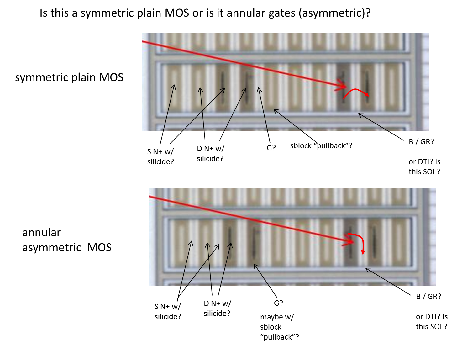
I use simple diode+RC-INV-bigFET to protect ESD for my IC. Diode+RC-INV-bigFET are from foundry standard IOS. Bad news is it cannot pass MM 200V test. Damage occurred at the first device in circuits, which is a switch, as below image shown , even though I do follow ESD rules. Seems my internal circuits are more susceptible to ESD stress.
Because I cannot revise the full chip, and the failure is marginal, i.e., can pass MM150V, but cannot pass MM200V, does it make sense to add PESD implant on the drain side of the switch to improve ESD by simply revising one mask layer?
Thank you all for your advice in advance!!