Continue to Site

Welcome to EDAboard.com

Welcome to our site! EDAboard.com is an international Electronics Discussion Forum focused on EDA software, circuits, schematics, books, theory, papers, asic, pld, 8051, DSP, Network, RF, Analog Design, PCB, Service Manuals... and a whole lot more! To participate you need to register. Registration is free. Click here to register now.

multiple SMPS noise problem

Status
Not open for further replies.

pasau

Newbie level 5
Joined
Feb 19, 2016
Messages
10
Helped
0
Reputation
0
Reaction score
0
Trophy points
1
Activity points
149
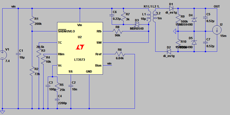
hi, i have an application that is powered by a 7.4V Li-Po battery. I use a flyback SMPS to generate a high voltage of 200V, and also some other DC converters to get 3V and -3V.

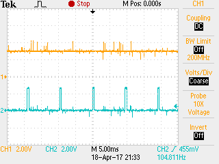
the low voltage powers some digital IC's. the problem is that the +- 3V line picks up way too much noise, i.e. around 4Vpp of noise, and is unusable. I get noise at the output of the +-3V supply even when the input is grounded.

I am searching for guidelines and advice on noise management for SMPS.

thanks and regards.
 

Just a little bit of ground noise can really bother current
mode controlled converters. If they are not in sync the
beat notes can be crazy; if in sync the ground and input
rail perturbation amplitude is at its worst. Maybe try a
few variations on input filter, separate the feed as far back
(common mode choke?) as practical?

Perhaps you'd be happier with a single pump and multiple
windings, if decent cross-regulation can be had.
 

Grounding is critical in SMPS supplies.
A single point ground that all the supplies connect to is usually preferable.
From there you run the grounds to the various circuits.
Did you do that in your configuration?

If that doesn't work then you may need to add some common-mode chokes at each SMPS output.
 

There is a piece of critical information missing:
Are the power supplies in the same or separate boards than the sensitive logic circuitry?
 

There is a piece of critical information missing:
Are the power supplies in the same or separate boards than the sensitive logic circuitry?

right now they are on separate board, since i am prototyping, but i want to have everything on a single board.
 

Hi,

To me it sounds like a measurement problem. Maybe just your scope probe pick up some noise.

But for sure it may be real noise.
Filters, GND wiring, shielding, twisted pair wires and a good PCB layout with solid GND planes will solve the problem.

For detailed assistance we need to see a photo of your circuits and it's wiring...and where you connected the scope probe..and we need to see scope pictures.

Klaus

Here are some pictures of my chaotic wiring, and the noise seen at the oscilloscope. and the 200V SMPS.

both this power supply and the 3V supply are powered by the same source, but they are both connected directly to the voltage source itself, in an attempt to minimize the noise from the parasitic inductance of the long wires. nonetheless, the signals on the scope are noisy. the waves are my 3V SMPS output, and a random signal.

So basically before i make a board with everything on it, i would like to know as much as possible what i can do to reduce noise from the switching current.

So far i noticed that plugging a different set of wires into the voltage source for both SMPS gives less noise, i.e. around 2vpp, which is better than it used to be if they take the same wire. And if i power them with a different voltage source for each, i get 1vpp, and only 0.75Vpp if i disconnect the output of the 200V supply, while using a different voltage source for both. So 0.75 is somehow picked up from the air. inductive coupling between adjacent wires maybe, idk.

As for filtering, im not exactly sure what to do. filter at the output of the 200V SMPS? is there some sort of guide for filtering SMPS noise?

thank you.

6700593100_1492569526.png


Hi,

Honestly...don't bother with noise...it simply is caused by the wiring.
If you want to avoid it, then you need a single PCB with a solid GND plane.
(At least this is the easiest way for good results).
Decoupling capacitors with very short traces to GND. For high current switching paths use multiple vias.

Usually in the switching regulator datasheets there are PCB layout recommendations.

Klaus
 

Status
Not open for further replies.

Similar threads

Part and Inventory Search

Welcome to EDABoard.com

Sponsor

Back
Top