niloufar-navidi
Junior Member level 1
Hi
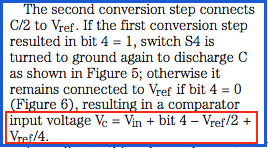
I cannot understand why in the comparison of the second MSB, Input voltage to the comparator would be :


While the charge on MSB has been discharged and there should be no Vref/2 anymore.
And vise versa , When MSB has not been discharged the input voltage to the comparator is:


While there should be a vref/2 in this formula.
The complete instruction: **broken link removed**
- - - Updated - - -
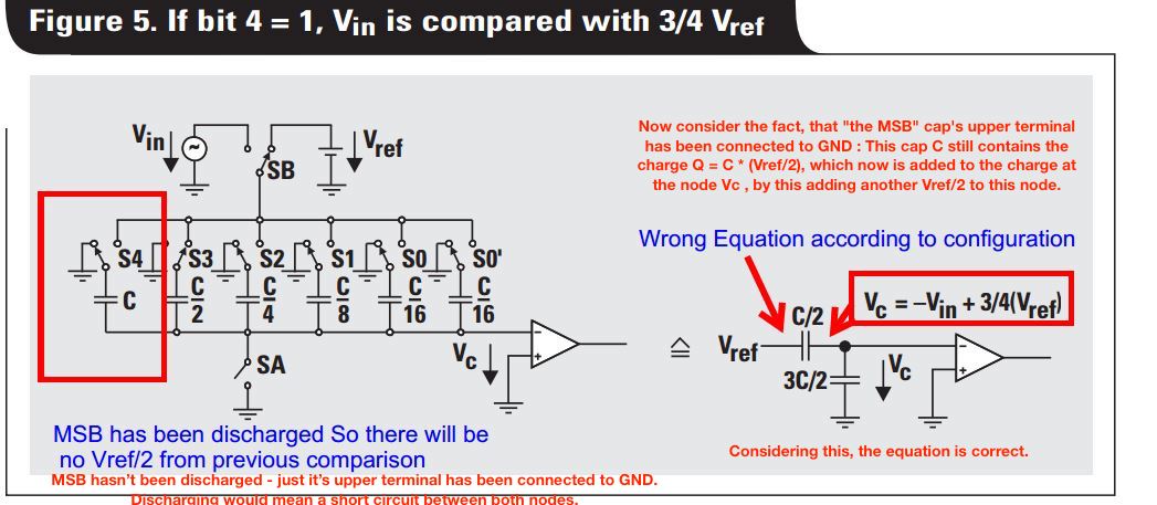
I think TI manual has got some problems, When MSB is 1 (bit4 here) and we are going to decide MSB/2, MSB cap should remain connected to vref!
I cannot understand why in the comparison of the second MSB, Input voltage to the comparator would be :
While the charge on MSB has been discharged and there should be no Vref/2 anymore.
And vise versa , When MSB has not been discharged the input voltage to the comparator is:
While there should be a vref/2 in this formula.
The complete instruction: **broken link removed**
- - - Updated - - -
I think TI manual has got some problems, When MSB is 1 (bit4 here) and we are going to decide MSB/2, MSB cap should remain connected to vref!
Last edited: