Continue to Site

Welcome to EDAboard.com

Welcome to our site! EDAboard.com is an international Electronics Discussion Forum focused on EDA software, circuits, schematics, books, theory, papers, asic, pld, 8051, DSP, Network, RF, Analog Design, PCB, Service Manuals... and a whole lot more! To participate you need to register. Registration is free. Click here to register now.

[SOLVED] Assura LVS errors about Unmatched Schematic Instance

Status
Not open for further replies.

19910219

Newbie level 4
Joined
Mar 29, 2017
Messages
6
Helped
0
Reputation
0
Reaction score
0
Trophy points
1
Activity points
58
HI folks.
I'm new for layout design and I'm facing the problem about Unmatched Schematic instances in LVS.

I generate every single MOSFET by "selected from source" and a part of them is on this problem.
I checked every pins of them and I thought they are all right. And When I click" ZOOM" in "Schematic Info" in "Devices Mismatch Tool". CDS.log shows "*WARNING* (GE-2133): The object XXXX does not exist in cellview pgchip/layoutsch/schematic. To create a probe, provide the name of an object that exists in the cellview.
Probed schematic device:/XXXX, no mapping to layout device"

BTW, I use 0.18um pdk from IBM.
Do you know what's this problem?
 

There's a device in the layout that your schematic
does not show. You should be able to select it by its
name in the extracted view and find the same X-Y
location in the layout view.

Maybe it's being "pruned" for being open or shorted.
 

Thanks for your reply. However, I'm still confused.

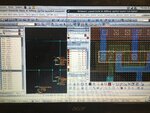
As you said, there's a device is not showed in schematic. But, I think it shows...Also, I can find it by click the device in layout ( and the device in schematic can be selected in the same time)..Also, the device name's showed in Navigator in schematic view..
And the device name can be found in netlist...
IMG_5973.jpg
 

Maybe the device is mismatched by type rather than
existence? Like (say) a lvt nmos in schematic and a
hvt nmos in layout? Depending on PDK you may have
the MOSFET varieties from a single "nmos" and would
get a parameter mismatch from that discrepancy, or
there could be lvtnmos and rvtnmos in which case
you would get a mismatched device.

I am confused by your description of the error and
behavior so these conjectures are only that.
 

I'd like to update this case.
Indeed, i don't know the reason that part of devices are not recognized in schematic view while I generate layout devices automatically( from schematic view) in layout view.
However, I tried to create a new project and new schematic ( re-draw the schematic I designed), also, I re-draw the layout without any changes. As a result,the LVS clears.
Maybe, it's fail because some data in old project is lost.
 

Status
Not open for further replies.

Part and Inventory Search

Welcome to EDABoard.com

Sponsor

Back
Top