saulbit
Member level 4
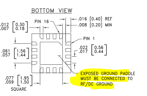
Hello everyone, I am working with a board for filter-switch bank, which consists of several spdt switches and four filters. The switch IC is HMC347LP3, from Hittite now a part of Analog Devices. The parameters in the datasheet of HMC347LP3 are very cool, including a 1.6dB typical insertion loss, a 44dB typical isolation. My schematic is about like this as follows:
Figure 1 Schematic of HMC347
and part of pcb is as follows (according to the ic designator U22 ):
Figure 2 part of pcb (U22)
The board material is RO4350B, with effective dielectric const of 3.48, and the 50 Ohm character resistance width is about 1.74mm. The ac-coupled capacitors are from ATC.
However, when I test the pcb in Fig.2 separately, I found the insertion loss is about 1.7dB for 8GHz, and about6dB for 10GHz, about 12dB for 12GHz, which is terrible for I used 4 switches, which would cause about 48dB loss for 12GHz. The loss of connector and test coaxes is subtracted. Referring to the isolation, which is only about 10dB for 12GHz.
What is wrong with the circuit? Can I achieve the parameters in the datasheet? or something is hided in the datasheet? What is the measuring method of datasheet parameters? The attachment is the datasheet of HMC347LP3. Any reply is appreciated. Thank you!
- - - Updated - - -
Last edited: