Continue to Site

Welcome to EDAboard.com

Welcome to our site! EDAboard.com is an international Electronics Discussion Forum focused on EDA software, circuits, schematics, books, theory, papers, asic, pld, 8051, DSP, Network, RF, Analog Design, PCB, Service Manuals... and a whole lot more! To participate you need to register. Registration is free. Click here to register now.

Through hole plating

Status
Not open for further replies.

gauravkothari23

Advanced Member level 2
Joined
Mar 21, 2015
Messages
640
Helped
5
Reputation
10
Reaction score
4
Trophy points
1,298
Activity points
6,922
hi all...
can anybody guide me for the through hole plating process for double sided PCB's. Till date i was using a wire and getting it soldered on both the sides of vias. but in some cases when the vias are placed under some SMD IC's, there is no possibilities of soldering the wire through the via under the SMD IC's. so i need to upgrade my PCB manufacturing process with through hole Plating.
can anybody let me how to through hole plate the PCB and what chemicals are used for the same.
 

The wire process works fine, but the circuit board has to be designed differently for them.
Solder the through holes before the IC's and sockets are placed on the board.
Don't put through holes under surface mount IC's because the solder bump will hold the IC up in the air.
Don't use the pins of sockets as vias, as the top side of the pins under the socket can't be soldered.
Design the board with a separate through hole connected to the socket pin. It can be under the socket, if
it doesn't interfere with the body of the socket by holding it up in the air.
Use a tight fitting wire in the through hole so that it doesn't slip when the second side is soldered.

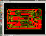
Attached is an image of an example pcb board designed with separate vias.
The vias are the pads marked with yellow circles.

Screenshot.png
 
Last edited:

Resist Etching of TPH.

hi all...
Till date i was making the double sided PCB with vias connecting using a wire. but now i have got a solution where i can get the hole conductive and now i dont have to use any wire into the vias. but my problem is how can i resist the through hole from getting etching when PCB is dipped into ferric chloride. i am using Photoresist dry film process to make double sided PCB. so basically my process is:
1) I drill my PCB
2) Make the holes Conductive.
3) Photo Exposure on both the side (Creating tracks and bridge over the holes using Photoresist film).
4) Etching.
5) Solder Mask using LPISM process.
but even after i expose the holes to UV light and try to create bridge over the holes to resist ferric chrolide enter the hole and etch the newly plated copper holes, the film over some of the holes also gets wiped out when the copper board is dipped into developer solution. what are the other ways where i can resist the holes from getting etch or any other ways where i can cover the holes.
 
Last edited by a moderator:

Status
Not open for further replies.

Part and Inventory Search

Welcome to EDABoard.com

Sponsor

Back
Top