CataM
Advanced Member level 4
- Joined
- Dec 23, 2015
- Messages
- 1,275
- Helped
- 314
- Reputation
- 628
- Reaction score
- 312
- Trophy points
- 83
- Location
- Madrid, Spain
- Activity points
- 8,409
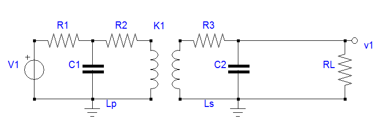
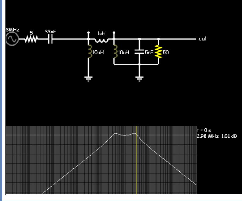
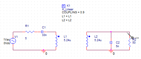
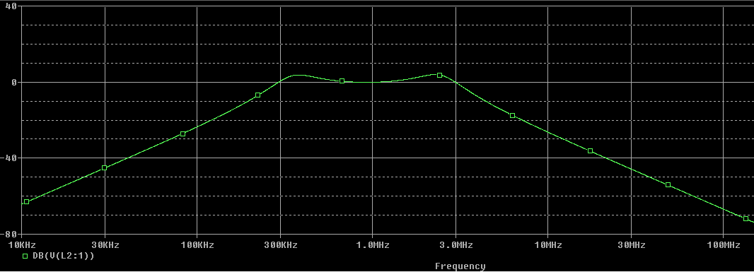
1)Which circuit have you used to make the bode plot from post #12. I have assumed the circuit used is the one in post #6, in which the red dashed line at the right means open circuit. Am I right ?(2) regarding the equivalent capacitance of the Rx side, there is another DC block cap connected to the output of the receiver, and then feed as the input of a logic inverter. This is the picture that showed in an earlier post in this treadView attachment 136867. I am using this inverter (https://www.ti.com/lit/ds/symlink/sn74lvc1g97.pdf).
My guess is, if we assume the Cgs of the input MOSFET of the inverter is still in pF level, Cgs will connect in series with this 10nF DC blocking cap, then stay in parallel with that 10nF cap C_SEC. So the overall load of the secondary data coil is still several pF level, like what you have pointed out, around 130pF. Is this analysis correct?
2)I will take the bold text in the above quote as a typo and think you wanted to say 10 pF.
3) You have to see the equivalent circuit of what you have after the "DC block capacitor" because I guess it does not end there. If you take the simple internal circuit of a CMOS inverter (one P channel and one N channel) and nothing else connected to its output i.e. with the drain of the CMOS inverter's ouput open, then the capacitance seen by the "DC block capacitor is" :
(Cgs1+Cgs2)//(Series of Cgd1+Cgd2 and Cds1+Cds2)