Continue to Site

Welcome to EDAboard.com

Welcome to our site! EDAboard.com is an international Electronics Discussion Forum focused on EDA software, circuits, schematics, books, theory, papers, asic, pld, 8051, DSP, Network, RF, Analog Design, PCB, Service Manuals... and a whole lot more! To participate you need to register. Registration is free. Click here to register now.

The error about ARAM reading

Status
Not open for further replies.

Kynix

Banned
Joined
Jun 27, 2016
Messages
24
Helped
0
Reputation
0
Reaction score
0
Trophy points
1
Activity points
0
Good afternoon~:-DI'm coming again! Thank you for taking time to read my thread.Today I'm also confusing about the FPGA. I hope someone in the forum can help me.:???:
I would like to ask the question about the reading of ARAM.
Please look at the following picture,when addr is 2, the dout should be 3.Why it appeared 1 here?
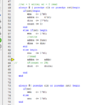
BRAM program.pngBRAM simulation.pngthe picture of BRAM simulation.png

Your help will be appreciated!
Wishes~:)
 

All BRAMs are synchronous, hence you get the data 1 clock after the address. ARAMs in FPGAs have to be built from logic and have low performance.
 

All BRAMs are synchronous, hence you get the data 1 clock after the address. ARAMs in FPGAs have to be built from logic and have low performance.

So...what do you mean? Can you explain it more clearly?
 

There are no asynchronous RAMs in an FPGA is that clear enough?

If you try to implement one it will either a) fail to implement, or b) end up as a huge design that implements latches in the LUT fabric to store bits.
 

Status
Not open for further replies.

Similar threads

Part and Inventory Search

Welcome to EDABoard.com

Sponsor

Back
Top