Continue to Site

Welcome to EDAboard.com

Welcome to our site! EDAboard.com is an international Electronics Discussion Forum focused on EDA software, circuits, schematics, books, theory, papers, asic, pld, 8051, DSP, Network, RF, Analog Design, PCB, Service Manuals... and a whole lot more! To participate you need to register. Registration is free. Click here to register now.

Seeking advice regarding structure of a DC-DC/PWM reg. for personal vaporizer.

Status
Not open for further replies.
Hmm, I have to read about DrMOS because I have never even heard of it.

Some things seems to be assumed that the user would know or understand(which probably is reasonable since I don't think that people like me is the usual user nor the intended target consumer) but an example would be the REFIN pins function.
All I can find out is that REFIN's function is "External reference voltage input for current sensing amplifier", and that it's absolute maximum rating is -0,3V up to VDD + 0,3V.
But what does that actually mean? Is it the voltage that supplies the opamp that is used to sense the current by some means, or is it a voltage that the output of the current sense opamp is scaled to, or is it something that simply limits how high the output voltage of the current sense amplifiers(whatever that is made out of) can get... I really don't understand the meaning of this pin and relevant to that is also that I don't know anything about the current sense output's range or meaning.

All that I can find out about the IOUT pin is that it's function is "Output of current sensing amplifier. V(IOUT) – V(REFIN) is proportional to the phase current.", but that doesn't tell me anything about how to interpret that voltage does it?
(VSW pin = Phase node connecting the HS MOSFET source and LS MOSFET drain – pin connection to the output inductor.)
"proportional" isn't worth anything if I don't know anything about at what ratio it is proportional, lets say that I am feeding 3V to REFIN, and the output during steady state operation of the converter is let's say 1V. What does that mean?

I looked up DrMOS quickly and I see that it establishes some sort of standard that any such device should adhere to in some aspects, I read this document which paints that picture at least.

When you say alternative to DrMOS, do you mean something that could replace DrMOS(while establishing it's own "rules" without regard for DrMOS) or do you mean something that is compatible with DrMOS?

- - - Updated - - -

Then I also wonder about the bandwidth of the current sense amplifier, how can I hope to utilize it... Can I count on it being able to supply pulse-pulse current information or is it more of an general output current figure...

Unless I find any more specific information about it I have to implement a separate current sensing circuit(which I might be forced to do even with that information depending on what that information says).
 

DrMOS chips are widely used to generate CPU 0.8 - 1.2 V core voltage from 12V power supply on PC motherboards, usually in multi-phase configuration. TI is apparently targeting the same market. Generally the devices are interesting for many low voltage/ high current applications.
 
  • Like
Reactions: David_

    David_

    Points: 2
    Helpful Answer Positive Rating
Hi,

After a quick look, how about reviewing literature related to the TPS53661, featured in the Application Schematic on page 5, in case it sheds some light on how to implement the IC? Another method is checking other manufacturer's datasheets for the same part, if they also make it, in case there are more detailed explanations in one.

Regarding the reference, it possibly/presumably means that a reference voltage - not a supply voltage - that, like most parts, can survive going beyond the rails by +/- 0.3V. "a voltage that the output of the current sense opamp is scaled to" - you would have thought so, without any additional info., presumably the current sense op amp senses a current converted to a voltage, which is compared to Vref/REFIN, and the difference appears as a voltage at Iout.

"3V to REFIN, and the output during steady state operation of the converter is let's say 1V. What does that mean?" - not sure if I've understood your meaning... The sensed current, phase flavour or not, should be unrelated to the converter output voltage. Probably not, but to me the current sense amplifier sounds - in essence - like an error amplifier, that - inventing facts I do not have - do something to modulate the duty cycle, maaaaybe.

To be honest, unless you can find reference designs, along with a datasheet that provides a few necessary formulas, and so on and suchlike, I'd already be looking at a different part that answers most preliminary questions in the datasheet, and doesn't look as though one may need three months of banging-head-on-various-walls-repeatedly research just to understand its implementation.
 
  • Like
Reactions: David_

    David_

    Points: 2
    Helpful Answer Positive Rating
After a quick look, how about reviewing literature related to the TPS53661, featured in the Application Schematic on page 5

That is a good idea, it didn't occur to me at all.

"3V to REFIN, and the output during steady state operation of the converter is let's say 1V. What does that mean?" - not sure if I've understood your meaning...

What I meant was that the datasheet revels absolutely nothing about the gain of the current sense amplifier, so if the current sense amplifier(pin IOUT) would under some condition output 1V that is completely worthless to me because for all I know that 1V is representing 1A sensed current, 100A sensed current or 32,7A sensed current...
 

Hi,

If there isn't any other material related to this IC, a very good option is to join the TI E2E community and post a question there in a relevant section.
 

I would choose another part and I am about to inspect all TI's similar ICs to see if any of them have more information.
The biggest problem though is that just as FvM wrote that these ICs are used for mostly(CPU 0.8 - 1.2 V core voltage) many and almost all of the ones I have looked at have according to there datasheet not been able to provide a output voltage above around 2,5V generally.

Now I have no idea where that limit is coming from(what would prevent such a IC to operate in such a way that the output was higher than 2,5V) but if the datasheet clearly specifies that the maximum output voltage is 2,5V then I assume that it is like that.
I have found 1 other IR component that supports higher outputs up to 5,5V but if it is used with output voltages above 2,5V then the internal current sensing function will not function and should be disregarded(current sense output connected to some specified potential like GND or VCC or similar).

So unless I find one that can output >=5V while using the current sensing then I might just as well use CSD95472 since I prefer that package over the others I have seen, it looks much easier to solder manually since it has pins along the outer edge of the package and then the entire underside apart from those pins consists of one very large GND pad where the IR packages feature the outer edge pins but then instead of having one single pad underneath they have 3-4 separate pads which seems as much more of a challenge to get soldered correctly given that I have no solder oven and are going to use a combination of a gas driven solder pen that have a hot air feature that is definitely capable of soldering as well as vias within the pad and I have planned to not cover them on the bottom side of the PCB and then by some means hold the IC against the PCB and take my solder iron and melt and heat the vias and cover them with solder so hopefully I can by those two means make sure that the large pad is properly soldered onto the footprint.

- - - Updated - - -

Hi,

If there isn't any other material related to this IC, a very good option is to join the TI E2E community and post a question there in a relevant section.

I don't know where my brain is at... TI E2E community... of course, why haven't I already been there...
I am a member.

Thanks
 

According to a app note I read it is only ceramic capacitors that are able to lower the input voltage ripple and hence input current ripple, but calculations says that in order to keep the input voltage ripple at a maximum of 75mV I will need 1333µF which I simply can't realize with ceramics.

100µF ceramics are available but I don't know what to do.

Using polymer caps with 9mΩ ESR I can get the required capacitanc with 1 or 2 such caps, and I wonder if perhaps I should get 2 * 100µF ceramics and put them as close to the input as possible and then place 1 or 2 polymer caps as close to them as possible(the polymers would ensure that the capacitance is high enough.

I am not sure that will do but on the other hand I don't see any other option.

- - - Updated - - -

Why 75mV?

The app note says that with 75mV and below the input current ripple will be manageable for the input capacitors.
 

I may have made the decision to change one aspect of the design which would change the circuit quite much.

Someone asked me on a other site "why use a filter if the frequency is 100 kHz? " and I don't know why I would use a filter.
I based the circuit concept on devices that operated on very low frequency switching, but if I am making a device that is switching at 100kHz then I can't imagine that it could matter if I filter it or not.

The only thing that makes me unsure about this is that I don't have a clear picture about how the regulation would be done, and as far as I can think about it it seems easier to control a buck output voltage rather than simply using unfiltered PWM while altering the duty-cycle.

No this is not a good idea I think as it is introducing the ever changing battery voltage into the picture again, which I don't think I would want to have to deal with in the software.
On the other hand it would make the hardware so much simpler and eliminate quite much space, so I will continue to ponder the idea.
 

You're finding out there's more than one way to construct your project.
* Single-ended DC vs alternating current
* filtered vs non-filtered
* constant duty cycle vs sine-PWM
Etc.

A truism comes to mind, one which applies to a lot of decisions we make in life: namely, No matter which you choose, there will be times you'll wonder if the other wouldn't have been a better choice.
 
  • Like
Reactions: David_

    David_

    Points: 2
    Helpful Answer Positive Rating
A truism comes to mind, one which applies to a lot of decisions we make in life: namely, No matter which you choose, there will be times you'll wonder if the other wouldn't have been a better choice.

It is almost universal; the option not selected and now unavailable always appear the better.

But the famous quote from Cardinal Newman seems to be apt here:

"Nothing would be done at all, if a man waited till he could do it so well, that no one could find fault with it"
 
No matter which you choose, there will be times you'll wonder if the other wouldn't have been a better choice.
Nothing would be done at all, if a man waited till he could do it so well, that no one could find fault with it

I think that is valuable to keep in mind, and since this doesn't have to be ideal I will go ahead and keep to the buck-converter design since that is what I wanted to learn about. Although I will make sure that I can easily attach a wire to the switch node somehow so that I am capable of trying the non filtered signal as well.

I had originally thought that I would etch a test PCB at home first but the design is more and more starting to look as it is relying on 4-layers being available which makes it hard to produce at home. But that don't have to be a problem given the prices for producing 4-layer PCBs today.

Unless I am mistake I only have the input and output capacitance to figure our before I can finish the board layout and get a prototype made, I think I have figured out the input capacitance so now I only have the output capacitance left and then I can start looking at the software, finally. But we'll see.
 

I have something I wonder if anyone have any opinion/theory about.

I have a 8,4V supply that is powering two synchronous buck-converters, one of the buck's need to be able to pass 40A while the other buck(which supplies all other kinds of circuits) will never output more than 300mA.

Since the circuit is using batteries that are charged externally, the high discharge rate of a device like this creates the need for two separate battery pairs so the device can be used all the time, one pair charging while the other pair is used. Which means that there will be lot's of battery changes, thus creating a need for reverse battery polarity protection.

I chose to go with what seems to be known as "the P-Ch MOSFET Trick", see the picture below.

But I don't prefer to protect that 40A converter that way since that would require a fancier PMOS and it would possibly generate quite a lot of extra heat, using that PMOS to protect that 300mA converter is perfect though.

PMOS_battery_reverse_polarity_protection_problem.png

What I am considering is whether or not that 40A buck converter needs protection, the positive battery rails sees a bunch of 100uF ceramic capacitors and the VIN pin of the CSD95373(or CSD95472, they are as good as identical except the 95373 doesn't have that unspecified current sensing circuit and have NotConnected pins instead). And what the VIN pin connects to is nothing more than the Drain of the high-side NMOS, the capacitors is of course the input capacitors.

So if the batteries are placed in the reverse direction then the PMOS will not conduct hence the circuits being fed by that 300mA converter isn't powered which means the MOSFET drivers in the CSD95373 isn't power nor receiving any PWM signal, then wouldn't both the MOSFETs(inside the CSD95373) Gates be floating, while the midpoint of the high-side and low-side NMOS's(switching node) isn't connected to anything and assumed floating as well.

The CSD95373's datasheet rates the VIN pin's allowed voltage as:

both VIN to PGND & VIN to VSW = -0,3V to +25V

Then shouldn't the VIN pin be okay with seeing -8,4V for a short amount of time(short "human" time not "µC" time)?


If I am to follow the datasheet exactly then I would put the CSD95373 behind the protecting PMOS, but I don't see why it should need that. I am okay with trying to expose a CSD95373 to the reverse battery voltage to see what happens, unless anyone here thinks there's a reason for why that is a bad idea.
 

Hi,

Is the reverse polarity protection PMOS backwards? The diode... I don't know, that circuit looks to me like as if it might protect the control circuitry but the buck converter MOSFET may allow the reverse voltage to go full circle, through the diode (the other one). No doubt I'm wrong.

I don't think there's any need to expose a part to the reverse voltage, when a simulation of that or a similar basic circuit might be quite enlightening as to what the reverse protection MOSFET will help with and what it may not.
 
  • Like
Reactions: David_

    David_

    Points: 2
    Helpful Answer Positive Rating
Is the reverse polarity protection PMOS backwards?

I guess it depends on how you view it, compared to a ordinary PMOS usage then I think it is backwards but this application counts on that being so.

See page 2 of this document.

I don't know why I seem to miss the obvious thing to do, I had not even consider trying to do a simulation to answer this question.
 

Seems O.K. the reverse polarity protection PMOSFET.

Beware of the 7.4 V VSG to fully turn on the PMOSFET. Consider a logic level PMOSFET and add a zener diode to clamp the VSG to 5 V.


I have to double check but I think I have selected a logic level PMOS which VGS rating is high enough so it can manage the full battery voltage so the zener isn't necessary.
 

I am facing a situation which I don't know how to handle, I am not even 100% sure it is a problem but I think this is one of those most basic layout problems which you don't want to make.

I often like to make my schematics with very unconventional stuff in order to illustrate to my self where the returns go and which components is critically connected to some point and so forth, the following schematic however is made purely for this post and the colours have meaning:

green = ordinary nets in eagle cad.
turquoise = VDD(the supply that powers the gate drives and logic within CSD95472)
purple = return for VDD
yellow = VIN supply(this is the supply that feeds the 40A synchronous buck-converter)
red = return for VIN

MOD_Return_issue.png

The CSD95472 have two PGND(I keep calling it PGND as it is called in it's datasheet but that doesn't indicate that there is another GND for other function in this package in this case) pins(one is a ordinary pin and the other is the large heat sink pad) and those two pins should be connected directly to each other. An alternative to the CSD95472 is the CSD95373 which is very similar, in the same package but without some of the pin functions that CSD95472 have, amongst other things the CSD95373 has only one PGND pin. I think I will go with the CSD95472 even though it is a little higher in cost its extra PGND pin makes the layout quite a bit easier.

But as the schematic tries to indicate, I have from the very start planned to route the return for the high-current buck-converter with it's very own GND path, but since the CSDWHATEVER requires a lower VDD voltage(lower than VIN in my case) that VDD is derived from a integrated buck converter, before going further let me tell you what that converter does.

The TPS62135 features a VSEL pin and two feedback connections(FB and FB2) FB2 are connected to GND through a NMOS that is controlled by VSEL. So while VSEL isn't activated the feedback voltage divider results in one output voltage which can then be changed by activating VSEL placing a second FB resistorlower in parallel with the first altering the feedback.

Which is an idea to be used like this:
The µC MCU is powered by the REG101(which has great PSRR ratings) set to 3,3V, REG101 can operate with very small drop-out voltages(which degrades it's performance) so when the device isn't actively being used the the µC setts the VSEL pin of TPS62135 so that it outputs a voltage above 3,3V but as close to that value as is safe to use. Then when the device are informed it is to activate and needs to perform analog-to-digital conversions, the µC makes the TPS62135 to increase it's output voltage into 5V which also brings that voltage into the range of what the CSD95472 requires(the CSD... is also controlled by a ENABLE signal) so so that the power loss due to the REG101 LDO is minimized.
Also the TPS62135 have a quite new operating function which makes it to automatically enter some low power mode when the output current is low, which really extends the converters efficiency at low currents.

And now I have gone through it all so the issue is that I want to keep the µC supply as clean as possible as that will also power current sense amplifier(s), maybe a differential amplifier and maybe even a ADC with an internal reference to enhance the resistance measurement compared to the µC's internal ADC.

So then I don't want to pass that 40A return through the ground of the TPS62135, but if I don't do that wouldn't I then create a ground loop?
 

Hi,

It looks as though you're using wires for the connections ;).

Wouldn't it be better to use separate layers for V+, GND, and signals? That way return paths are as short as possible (recommended), and I believe that an uninterrupted ground plane means everything's at an equal potential/ground reference. Long paths create big loops, I think. You can make small horseshoe-shaped borders around the sensitive ICs GND pins which supposedly cushion them a little from whatever else is happening on the board.

Have you read this, maybe not applicable, but interesting enough.

View attachment Decoupling, Grounding, and Making Things Go Right for a Change AN-202.pdf
 
  • Like
Reactions: David_

    David_

    Points: 2
    Helpful Answer Positive Rating
This is the furthest into a 4-layer design I have gotten and I think it may be the case that I have problems imagining the layout, but we'll see.

It doesn't sound as you are thinking what I thought might be a problem to be a problem.
What I was thinking about is that the CSD95472 have two supplies, one 5V supply for the digital and driver stuff and then the raw battery voltage while in essence only one GND connection(it has two but they are directly connected on the PCB, 0,5mm between them)
I want to route the high-current paths away from all the other supplies powered by the battery so those currents doesn't disturb those supplies that are feeding possibly noise sensitive circuits.

But the IC that is passing that 40A current is also receiving 5V from a regulator that also powers those noise sensitive circuits, is it OK to tie that CSD95472 to GND in two places, first a high-current GND path back to the battery and then a low-current path back to the output capacitor of the regulator generating that 5V?

Or is that creating a ground loop or might it cause some other ill effect?

Since 5V supply to the CSD95472 is quite low, a few mA maybe a couple of 10's of mA. Could it still be a problem to route it like this:
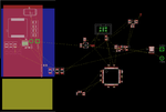
This is a very quick illustration in paint in which I have put circles to indicate where the different circuit areas are located and I have shifted them to more illustrate my point. After that picture come a picture of how I have planned my PCB and its size.
return ok.pngmod layout.png
In the eagle picture, the white line is the PCBs boarder that is what I have hopped will be the absolute maximum dimensions, 2 * 4 inch.

Oh I forgot to one thing in the paint picture, it was going to show a supply connection running from the yellow circle directly to the red circle,which would then return to the battery and back to the yellow circle.

I know such routing is not good but could it be just "OK" without inducing a lot of noise given the low current amplitude, does anyone have any thoughts/opinions about that?
 

Hi,

I don't know the answer to several of your questions, but one suggestion is - space permitting - to use a separate regulator for each function: one for high current and another for noise sensitive, the same as is recommended for (analog) circuits with clock-type ICs.
 
  • Like
Reactions: David_

    David_

    Points: 2
    Helpful Answer Positive Rating
Status
Not open for further replies.

Part and Inventory Search

Welcome to EDABoard.com

Sponsor

Back
Top