beginner_EDA
Full Member level 4
Hi,
I am trying to understand 7 series Transceiver for Kintex xc7k325tffg900-2 FPGA.
https://www.xilinx.com/support/documentation/user_guides/ug476_7Series_Transceivers.pdf
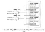
In my project i would like to use configuration as in attachment.
In the project LMH1983
https://www.ti.com/lit/ds/symlink/lmh1983.pdf
has been used which generate 3 clocks. 148.5 MHz, 148.35 MHz and 27 MHz.
Similarly Si5324
https://www.silabs.com/Support Documents/TechnicalDocs/Si5324.pdf
has been used which generates 156.25 MHz clock and controlled by I2C bus.
148.5 MHz clock from LMH1983 goes to gtxe2_i(GTXE2_COMMON) and 148.35 MHz from LMH1983 goes to gtxe2_i(GTXE2_CHANNEL) of Transceiver. This is for SDI.
27 MHZ clock from LMH1983 goes into a process which controls I2C bus and generates 156.25 MHz clock from Si5324.This 156.25 MHz clock goes into another Transceiver. This is for 10 Gig pcspma.
I am trying to understand these clocks and Transceiver relation and how they are arranged and unfortunately have no success.
I would like to know could anybody please calrify me the main steps which should be followed to use 7 Series Transceiver in a project. Ug476 seems to me as an Ocean and difficult to understand. It would be great if somebody clarify the concept.
I am trying to understand 7 series Transceiver for Kintex xc7k325tffg900-2 FPGA.
https://www.xilinx.com/support/documentation/user_guides/ug476_7Series_Transceivers.pdf
In my project i would like to use configuration as in attachment.
In the project LMH1983
https://www.ti.com/lit/ds/symlink/lmh1983.pdf
has been used which generate 3 clocks. 148.5 MHz, 148.35 MHz and 27 MHz.
Similarly Si5324
https://www.silabs.com/Support Documents/TechnicalDocs/Si5324.pdf
has been used which generates 156.25 MHz clock and controlled by I2C bus.
148.5 MHz clock from LMH1983 goes to gtxe2_i(GTXE2_COMMON) and 148.35 MHz from LMH1983 goes to gtxe2_i(GTXE2_CHANNEL) of Transceiver. This is for SDI.
27 MHZ clock from LMH1983 goes into a process which controls I2C bus and generates 156.25 MHz clock from Si5324.This 156.25 MHz clock goes into another Transceiver. This is for 10 Gig pcspma.
I am trying to understand these clocks and Transceiver relation and how they are arranged and unfortunately have no success.
I would like to know could anybody please calrify me the main steps which should be followed to use 7 Series Transceiver in a project. Ug476 seems to me as an Ocean and difficult to understand. It would be great if somebody clarify the concept.
Attachments
Last edited: