Continue to Site

Welcome to EDAboard.com

Welcome to our site! EDAboard.com is an international Electronics Discussion Forum focused on EDA software, circuits, schematics, books, theory, papers, asic, pld, 8051, DSP, Network, RF, Analog Design, PCB, Service Manuals... and a whole lot more! To participate you need to register. Registration is free. Click here to register now.

PCB trace width vs. heat

Status
Not open for further replies.

juz_ad

Full Member level 2
Joined
Dec 17, 2011
Messages
130
Helped
0
Reputation
0
Reaction score
0
Trophy points
1,296
Activity points
2,541
Apologies if I'm way off the mark here - trying to understand some PCB heat issues...
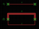
Screen Shot 2016-10-06 at 20.03.57.png

1) I understand that if a given trace width is too thin (A) to dissipate the amount of current/heat it needs to carry - it will get hot.

2) If the trace took two paths - one (B) with a width that would adequately dissipate the required heat for that trace and one (C) that was still too thin - would trace (B) compensate at all for the temperature of trace (C) - or would trace (C) still get just as hot?

I understand this is a really basic example and there's load of other real-world variables - hope the question makes sense.

Thanks,

/ J
 

Think of the traces as resistances (which, in fact, they are). Most of the current will flow through the fat trace.
 
  • Like
Reactions: juz_ad

    juz_ad

    Points: 2
    Helpful Answer Positive Rating
In addition, if the trace is undersized, another way of understand it could be as heatsinks, where the surface matter, namely a coarse trace tend to have a lower power rating if compared to the same thickness divided into thinner tracks with a reasonable clearance.
 

Hello juz_ad,
The rule I follow when making my PCB's is to ensure that my track widths in my power supply are adequate to distribute current throughout the circuit.
Thinner tracks can be used for integrated circuits, as an example, that consume quite a bit less current than your power supply.
The main thing is that you make sure that your track widths within the supply are enough to cater for the rest of the circuit, as this will dissipate the most amount of heat, and the lower current paths will dissipate their own heat for their requirements.
Another way to improve the current rating of a track is to have it exposed and you do a manual solder pour onto it.
A word of warning here: If you want to use heavy tracks for your initial current distribution +3Amps, as an example, you MUST make sure your ground tracks are the same width/s as well.
I hope the above helps.
Regards,
Relayer
 
  • Like
Reactions: juz_ad

    juz_ad

    Points: 2
    Helpful Answer Positive Rating
Think of the traces as resistances (which, in fact, they are). Most of the current will flow through the fat trace.
So - if there's a wider/thicker, less resistive trace for current to flow through - it will take that, which would potentially mean less current travelling through the thinner, more resistive trace - which would mean less heat on that trace.
Assuming I've understood that - it makes sense. It's basically following the path of least resistance.
Thanks.
 

Hi,

It sounds that thinner traces means less heat. This not true.

You need low overall resistance to carry high current.

--> Use wide, thick and short traces.

Klaus
 

It sounds that thinner traces means less heat. This not true.

Wider traces == less resistance == less heat (in very basic terms).

Yes - that was the intention of my original post.

Thanks for the clarification though.

/ J
 

Status
Not open for further replies.

Part and Inventory Search

Welcome to EDABoard.com

Sponsor

Back
Top