Continue to Site

Welcome to EDAboard.com

Welcome to our site! EDAboard.com is an international Electronics Discussion Forum focused on EDA software, circuits, schematics, books, theory, papers, asic, pld, 8051, DSP, Network, RF, Analog Design, PCB, Service Manuals... and a whole lot more! To participate you need to register. Registration is free. Click here to register now.

PCB shielding ground connection

Status
Not open for further replies.

aaron_do

Member level 3
Joined
Dec 12, 2007
Messages
64
Helped
4
Reputation
8
Reaction score
3
Trophy points
1,288
Activity points
1,878
Hi all,


my questions is what is the best way to shield a PCB? Assume I have bottom and top metal covers for my PCB. My PCB has a ground plane. Should my shield simply connect to the ground plane all around the edge of the PCB? The alternative is to have a ring of metal around the edge of the PCB with vias through the PCB to form a kind of side wall. This side wall would connect to the PCB ground at only one point on the PCB, and my top and bottom shield covers would be soldered to the shield. I suppose I could also not connect the shield to ground at all...

Which option is better, and which is more commonly done in practice? I have seen several designs which only have a top cover, and I believe the PCB ground plane forms the bottom of the metal box. My understanding is that this isn't really optimal as the currents flowing in the PCB ground plane will result in fields outside the box, and also make the inside of the box susceptible to fields on the outside.

Any comments are welcome.


thanks,
Aaron
 

Yes, ideally would to use only the top cover shield, and at the bottom to use a solid ground on the PCB layer.
The trend now designing RF circuits (with whatever complexity) is to don't use a shield at all. This would place a lot of pressure on the layout and system designers.
Theoretically if all the circuits are well matched, well decoupled, with proper signal levels, and using good grounding and tracing on the PCB layout, you don't need any shield.
 
The top metal cover shields all components below from external EM interferences; as modern components have shrunk in size, this effect has gone down rather significantly. As vfone has remarked, a well designed system does not radiate much and is rather immune to external induced signals. If you have lots of open capacitors and inductors, you are required to use a shield and this may even be floating.
 
Depends what this is.

If its a high speed digital circuit, or video, with external ground and power planes, it probably does not need anything else as all the tracks are sandwiched between the planes.

If its a radio circuit of either high RF power, or of high RF sensitivity, and there are "hot" components mounted outside the planes, then external shielding will probably be required.

You can solder the shields directly onto the board, which becomes a maintenance nightmare, or if practical, place the whole board into a shielded metal enclosure which might be a conveniently removable sub assembly of the main equipment.

Quite a few choices, and it all works if well thought through.
Spare a thought for the poor maintenance guy !
It must be either very easy to get into, or quick to replace as a whole assembly if not.
 
thanks for all the replies.

I'm more interested in the grounding of the shield. vfone has agreed that the shield should be connected solidly to the ground plane which lies underneath the RF circuitry (if I understood correctly). c_mitra also mentioned that the shield can be floating.

So what are the pros and cons of floating vs connected to the ground plane? Honestly I haven't really seen any floating shields connected directly to the PCB. On the other hand, I have read that a proper shield is supposed to be floating...


thanks,
Aaron
 

c_mitra also mentioned that the shield can be floating.

The Shield just works like a Faraday cage; If you have ground plane on the bottom side of the PCB, please connect the shield by all means to the ground plane. But puritans will cry: why you are making a ground loop when we can live without one? How does it matter?

Nobody knows about the circuit and the layout more than you and it will be your decision. For perfect protection, the Faraday cage must be fully enclosed.
 

It depends on the frequencies involved.

If the frequencies are low, and the metal screen cover fairly small, then single point grounding will probably work fine.

These days we now have things working up at several Ghz, and that requires pretty solid all around bonding to be really effective. Definitely no long slots.

Your best bet might be to eyeball similar equipment made by other reputable companies, and see how they went about it.
 

Your best bet might be to eyeball similar equipment made by other reputable companies, and see how they went about it.

That's what I did, and that's why I'm asking my questions. What I noted is that products are designed with the top shield solidly connected to the bottom ground plane. On the other hand, my reading tells me that an effective shield only has one ground connection.

- - - Updated - - -

The Shield just works like a Faraday cage; If you have ground plane on the bottom side of the PCB, please connect the shield by all means to the ground plane. But puritans will cry: why you are making a ground loop when we can live without one? How does it matter?

Nobody knows about the circuit and the layout more than you and it will be your decision. For perfect protection, the Faraday cage must be fully enclosed.

I want the "cage" to be fully enclosed, but if I have a bottom shield, then I have two possibilities:

1) Connect the top shield to the bottom ground plane.
2) Connect the top shield to the bottom shield, and only connect the cage to the PCB ground at one point.

so which is preferable? I fully intend to make the final decision, but I'm hoping for some advise first....


thanks,
Aaron
 

I believe we don't have sufficient information to answer the question.

Consider that an enclosure entirely connected to the internal ground plane is a classical RF instrument design concept. You can expect a small residual coupling between ground plane and the outside. In case of extreme shielding requirements, a double screen may be required.

Having the internal ground plane connected to the shielding enclosure in a single point can promote ground plane modes and return currents due to internal coupling. At the end of the day, shielding isolation may be even reduced.

In case of doubt, perform EM simulations of the full structure.
 
It depends on the frequencies involved.

At 3GHz, your wavelength is 10cm and lambda/2 is 5cm. A circuit element of length 5cm in the correct orientation and polarization will act as an antenna and maximum voltage will be induced (across this component). Typical electronic components are approx at least 10 times smaller and the voltage induced will be correspondingly less.

The story will be different with the ground plane; different points on the ground plane will be seen at different potential (unless you get into the real mess of collecting all the ground connections at one point) and in reality the ground plane too needs some protection.
 

I should have used lambda/4 rather than lambda/2. That is the distance from the node to the antinode.
 

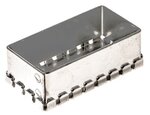
I believe you can buy these screening boxes in various sizes that can be soldered direct to a copper ground plane. The ones I have seen come with a removable lid held solidly in position by multiple springy fingers.

screenbox.jpg

Small holes between the fingers are not a problem. Its long slots you need to avoid.
 

I believe we don't have sufficient information to answer the question.

Consider that an enclosure entirely connected to the internal ground plane is a classical RF instrument design concept. You can expect a small residual coupling between ground plane and the outside. In case of extreme shielding requirements, a double screen may be required.

Having the internal ground plane connected to the shielding enclosure in a single point can promote ground plane modes and return currents due to internal coupling. At the end of the day, shielding isolation may be even reduced.

In case of doubt, perform EM simulations of the full structure.

thanks for the reply. So what I'm thinking is that when you have a top shield connected solidly to the bottom ground plane, then any forward signal path will have its return path in the ground plane, and hence, in the bottom of the shield. The loop inductance formed between the forward path and the bottom shield will result in magnetic field beneath the bottom shield cover.

For the second case, the metal shield is only connected at one point to the bottom ground plane. Now my EM theory is not very good, but I think the electric field will be zero outside the shield. What about the magnetic field? My thinking is that if there are eddy currents induced in the shield, then these eddy currents will produce a field which will counter the ground plane's magnetic field resulting in zero magnetic field outside the shield.

Please correct me if I'm wrong.


thanks,
Aaron
 

That is my understanding too, that a non ferrous shield (copper, aluminium) works by having induced eddy currents oppose the magnetic field trying to pass through the screen.
In effect an efficient shorted turn.
And also a direct enclosed Faraday screen blocking the electric fields.

For this to work the screen needs to be completely passive.
It should not ideally have voltages or currents forced into the shielding by multiple connection points to active internal circuitry.

Its a similar philosophical concept to an equipotential earthing system.
Where the earth must NEVER also double as a current carrying power return.

But we need to be realistic.

A distributed ground plane with a few CMOS ICs or some low level amplifiers will not generate enough circulating current into the ground plane to have much effect.

Some kind of extreme power amplifier is a whole different thing.

Ok. I got ur point. Thanks!
 

I insist on the consideration that depending on the frequency range of interest, other effects superimpose your simple concept. E.g. standing waves inside the shielding create a different coupling mechanism. That's why we have usually shield tied to ground plane in RF instruments.

I still fear that a discussion abstracting from application details is of limited use.
 
That is my understanding too, that a non ferrous shield (copper, aluminium) works by having induced eddy currents oppose the magnetic field trying to pass through the screen.
In effect an efficient shorted turn.
And also a direct enclosed Faraday screen blocking the electric fields.

For this to work the screen needs to be completely passive.
It should not ideally have voltages or currents forced into the shielding by multiple connection points to active internal circuitry.

There are multiple effects. A metal (electrically conducting) enclosure is always at a constant potential. If all the points on the surface of the enclosure are at the same potential, the electric field inside the enclosure is ZERO.

If the surface potential is not constant, it will be associated with an electric current. This current will have a magnetic field associated with it and the changing magnetic field is going to induce the eddy currents that will oppose the original magnetic field. This cancellation is never going to be perfect but can be reduced to any insignificant level by proper design.

It is the same way earth's magnetic field is produced by the magnetic elements in the core of the earth and circulating electric currents, acting like a solenoid, up in the atmosphere. Whenever we teach students in the theory, we tell that the potential is always zero at infinity by definition (without elaborating) and when we teach the engineers, we say that the potential at the earth's surface is zero (again without elaborating). All instruments are grounded to prevent electrical shock and all current return paths are called ground by convention. It will still be ground while flying in a plane!!

- - - Updated - - -

Now my EM theory is not very good, but I think the electric field will be zero outside the shield. What about the magnetic field? My thinking is that if there are eddy currents induced in the shield, then these eddy currents will produce a field which will counter the ground plane's magnetic field resulting in zero magnetic field outside the shield.

If a region is enclosed by an equipotential surface, the electric field inside the enclosed region is zero. The problem becomes when the potential of the equipotential surface is changing. Hell breaks loose!

if you change the potential so slowly that the surface always stays at the same potential, then nothing to worry. The problem is when the potential changes so fast that different points of the surface of the enclosure are at different potentials at different times... This causes current to flow and generate electromagnetic effects.

The magnetic field induced by the eddy currents will never be able to completely counter the external cause. (perhaps not true for superconductors but that is a different story)

In summary, it is very easy to remove a static electric field but impossible to remove a changing electric field.
 
I insist on the consideration that depending on the frequency range of interest, other effects superimpose your simple concept. E.g. standing waves inside the shielding create a different coupling mechanism. That's why we have usually shield tied to ground plane in RF instruments.

I still fear that a discussion abstracting from application details is of limited use.

Absolutely !
We might be talking about screening at 50 Hz.
Or is it at 50 Ghz ?

Are we trying to keep stuff in, or keep stuff out of our magic box ?
The best approach to the problem can vary hugely.
 

I insist on the consideration that depending on the frequency range of interest, other effects superimpose your simple concept. E.g. standing waves inside the shielding create a different coupling mechanism. That's why we have usually shield tied to ground plane in RF instruments.

I still fear that a discussion abstracting from application details is of limited use.

OK. Lets take for example, an RF circuit which has power in the 100MHz to 50GHz range, and the unit's dimensions are somewhere between 2cm and 10cm in length. Obviously there is a big difference between 100MHz and 50GHz, so I would love to hear the difference in shield considerations.

BTW, do you have any reading you would suggest? My background is more on the electronics side of RF, but the EM side interests me.

thanks,
Aaron

- - - Updated - - -

This cancellation is never going to be perfect but can be reduced to any insignificant level by proper design.

Can you recommend any reading on proper design methods?

thanks,
Aaron
 

Best current reference on the whole EMC topic is:

"Electromagnetic compatibility engineering" by Henry Ott.

Six hundred pages, and not exactly low cost new.
But pretty good value second hand.

It has now become a standard reference University course text that you will find at any University book shop or library.

Shielding and screening extremely well covered.

https://www.amazon.com/Electromagne...rds=electromagnetic+compatibility+engineering
 
Status
Not open for further replies.

Part and Inventory Search

Welcome to EDABoard.com

Sponsor

Back
Top