Continue to Site

Welcome to EDAboard.com

Welcome to our site! EDAboard.com is an international Electronics Discussion Forum focused on EDA software, circuits, schematics, books, theory, papers, asic, pld, 8051, DSP, Network, RF, Analog Design, PCB, Service Manuals... and a whole lot more! To participate you need to register. Registration is free. Click here to register now.

Operating point in MOSFET differential pair with current mirror and current source

Status
Not open for further replies.

farhan89

Junior Member level 3
Joined
Jul 29, 2011
Messages
26
Helped
0
Reputation
0
Reaction score
0
Trophy points
1,281
Activity points
1,517
Hello,

I am simulating differential pair with current mirror and current source (attached image , top is with current source and bottom with current mirror configuration) and I have confusion regarding operating point. I am following Electronics circuits book by tietze and schenk and there it is described that these configurations cannot be used direct for calculating differential and common mode gain with open ended output. For proper operating point a large inductor i.e. 10^9 should be connected at output with a voltage source. I am confused what changes will this bring to the circuit simulation.
Any suggestions or hints for solution ?

Thanks
diff.JPG
 

The long-tail pair is the basis for a differential amplifier. Try starting with only that. Put resistors where you have T3-4-5.

You still need to find the proper operating point. Adjust the resistor values, until you get the output voltage to change in response to small changes in bias voltage. (This process is identical to what we need to do to find a lone transistor's proper operating point.)

After you gain success, try adding the current mirrors and current sources.
 
... For proper operating point a large inductor i.e. 10^9 should be connected at output with a voltage source. I am confused what changes will this bring to the circuit simulation.

As said in the following text (by Tietze-Schenk), this is a method for simulation to keep the outputs (of a fully differential amplifier) at their required DC operation points, without deteriorating their ac behavior too much because of the huge inductances. In reality this is achieved by a CMFB circuit, which compares the output voltages with a DC reference voltage and controls the current sources accordingly.

For simulation purpose the former method is simpler, as it needs only 2 inductances and the DC reference voltage source.
 
As said in the following text (by Tietze-Schenk), this is a method for simulation to keep the outputs (of a fully differential amplifier) at their required DC operation points, without deteriorating their ac behavior too much because of the huge inductances. In reality this is achieved by a CMFB circuit, which compares the output voltages with a DC reference voltage and controls the current sources accordingly.

For simulation purpose the former method is simpler, as it needs only 2 inductance and the DC reference voltage source.

Hey, Thank you for the explanation. if I am not wrong then by DC reference voltage source you mean to attach a voltage source after the inductor and the DC source voltage has the same value as the drain voltage at differential pair transistor ?
 
Last edited:

if I am not wrong then by DC reference voltage source you mean to attach a voltage source after the inductor and the DC source voltage has the same value as the drain voltage at differential pair transistor ?
Right. And its the same voltage value as the reference voltage value of CMFB circuits.
 
Right. And its the same voltage value as the reference voltage value of CMFB circuits.

Thanks, I have one more confusion, I tried to simulate the top design (shown in main post schematic), but the gain is very low. I noticed that the DC operating points seems to be incorrect.
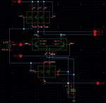
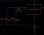
diff_sch.JPGdifft_tb.JPG

I have setup the schematic and test bench shown in images. The problem is the upper PMOS sources VDS is very low , VDD is 3.3 V and voltages at the drain of differential pair is around 3.2 volts. It doesnt seems to be correct to me . Is this due to the gate voltage at PMOS sources ?.
 

... The problem is the upper PMOS sources VDS is very low , VDD is 3.3 V and voltages at the drain of differential pair is around 3.2 volts. It doesnt seems to be correct to me . Is this due to the gate voltage at PMOS sources ?.

Yes, I think so. Try lower W/L ratio at the PMOS transistors - or higher W/L at the diff pair - this should also give you better gain.
 
Yes, I think so. Try lower W/L ratio at the PMOS transistors - or higher W/L at the diff pair - this should also give you better gain.

Hey, Thank for your help!
The problem was with the mirror ratio of tail current source, I used the ratio of 1 instead of 2. I have simulated this design by fixing the common mode DC voltage and sweeping differential voltage from -0.3V to +3V and tail current is approx 2.2 uA (1.1 uA for each branch) and obtained the gain of around 23 dB and with the increase in W/L of diff pair the gain also increases but I am confused related to my DC simulations plot. When I plot the output voltage and current curves, the output voltage curves doesn't look ' symmetric to me . Please see the attached images for the voltages and current curves.
diffpairI.JPGdiffpairV.JPG

Are the voltages curves correct because I see that the voltages at lower levels(VOUT2 at -0.3 V, VOUT1 at +0.3V) are not constant. and I have one more question that what are the typical values of small signal differential and common mode gain for differential amplifier with current sources and differential amplifier with current mirror load.

Thanks
 

... the output voltage curves doesn't look ' symmetric to me . Please see the attached images for the voltages and current curves.
Are the voltages curves correct because I see that the voltages at lower levels(VOUT2 at -0.3 V, VOUT1 at +0.3V) are not constant.
I think they are very symmetric. Try and mirror one curve!

I have one more question that what are the typical values of small signal differential and common mode gain for differential amplifier with current sources and differential amplifier with current mirror load.
Don't know, sorry, I'd have to search for examples myself.
 

Status
Not open for further replies.

Part and Inventory Search

Welcome to EDABoard.com

Sponsor

Back
Top