Continue to Site

Welcome to EDAboard.com

Welcome to our site! EDAboard.com is an international Electronics Discussion Forum focused on EDA software, circuits, schematics, books, theory, papers, asic, pld, 8051, DSP, Network, RF, Analog Design, PCB, Service Manuals... and a whole lot more! To participate you need to register. Registration is free. Click here to register now.

CMOS bridge inverter with inductive load

Status
Not open for further replies.

pal114525

Member level 5
Joined
May 20, 2015
Messages
87
Helped
0
Reputation
0
Reaction score
0
Trophy points
6
Activity points
717
Hi,

Please see the attached schematic.
Would you be kind to explain me the following points?

1. How to remove the distortion from the Vosc output?
2. How can I enhance the sinusoidal current through the inductor/coil?

Thanks & Regards.
 

Attachments

  • H-bridge.png
    H-bridge.png
    110.3 KB · Views: 94

The phase shift oscillator is not resonant with the load (11.2 kHz Q=3 )
Can you tune the oscillator or do you prefer to resonate with the load instead.
 

1. How to remove the distortion from the Vosc output?
Why do you worry this small distortion? Did you already monitor the bridge output voltages? Did you look at the transistor currents?

That's a failed attempt to make a woking inverter circuit.

Nevertheless you get an almost sinusoidal current with squarewave drive, so it shows some options how an inverter may be designed.
 

Here is a simple way to make an op amp detect the resonant frequency of the series LCR, and in turn drive it at that same frequency, thus automatically generating a sinewave across the load.


Oscillations are self-starting in simulation.
 

Hi,

Thanks for your valuable feedback.
Here, 10ohm resistor is the internal resistance of the coil.

Would you be kind to explain me the following point?

1. What the functionality of 10m ohm resistor in the circuit?
2. What are the purposes of using C1 and C2 along with the resistors in parallel.

Thanks & Regards.
 

I'm not sure if the circuit presented by BradtheRad is a better solution for your problem. It only attempts to solve a specific point, operate the circuit at the actual resonance frequency of the load circuit.

Both circuits suffer from low efficiency and overlapping conduction of bridge output transistors. It may be reasonable to state first what you want to achieve.
 

Hi,

Thanks for your valuable feedback.

I want to pass a sinusoidal current through a coil having inductance 450uH and internal resistance of ~10ohm. This signal should have a frequency of around 16KHz.
So that it can create an EM field.

Thanks & Regards.
 

There are two options:

- drive the H-bridge with 0/12V square waves. This gives slightly distorted output current, but still a kind of sine waveform
- design a linear bridge amplifier that feeds a true sine voltage to the LC circuit if you rely on very low distortion
 

At Brad, there is a wee error in your schematic above, as drawn the two transistors will turn on and short the 12V supply, it appears the sim does not show this - it should...
 

the two transistors will turn on and short the 12V supply, it appears the sim does not show this - it should...
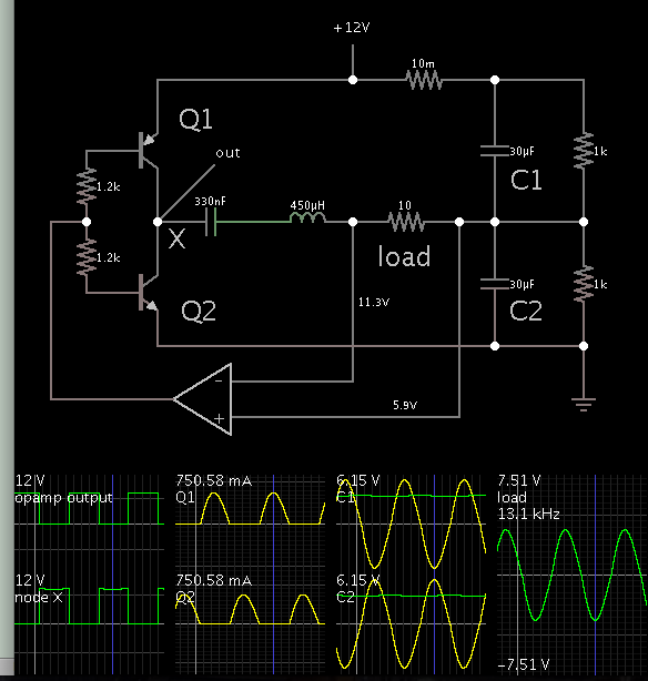
In a very idealized simulation circuit, bridge shoot-through may be avoided. But that's surely not a template for a real design.

I also have to correct my previous statement about this circuit. Theoretically, the transistors are driving a squarewave. In so far it's what you want. But you would provide locking and deadtime generation in a real circuit.
 

But you would provide locking and deadtime generation in a real circuit.

Hi,

Thanks for your valuable feedback.
Would you please explain me what is locking time and dead time in real circuit?

Thanks & Regards.
 

"Locking" means that the circuit avoids simultaneous turn-on of high- and low-side transistor by design.

A deadtime with both transistors turned-off is usually added to delay transistor turn-on until the current fall-time of the previously conducting transistor has elapsed. For MOSFETs, usual deadtimes are in 10 to a few 100 ns range, for bipolar transistors up to a few µs.
 

Hi,

Thanks for your valuable feedback.
Here, 10ohm resistor is the internal resistance of the coil.

Would you be kind to explain me the following point?

1. What the functionality of 10m ohm resistor in the circuit?
2. What are the purposes of using C1 and C2 along with the resistors in parallel.

Thanks & Regards.

C1 and C2 are an easy way to allow the half-bridge (at left) to act as a full H-bridge. The capacitors establish a node, midway between VCC and 0V ground.

The 10m resistor would be unnecessary except that the simulator calls it an error to place capacitors in series.

My simulation is chiefly good for demonstrating how a concept might work. There were many arrangements which I tried but which did not work. Such as which component to measure the differential voltage, what sequence the LCR components should be, which input and output specs work for the op amp. Etc.

I found that the op amp responds properly when it senses voltage transitions across the resistor. This can be a small ohm value, inline with your inductor.

Your schematic has a full H-bridge. This is preferable over my schematic, if you wish to drive greater current through the LCR. However your control circuit will need to be more complex.

My circuit can go into stagnation. This will allow severe shoot-through. You may need to set some amount of dead time (as implied in post #9). You may need to use two or more separate control devices. Etc.

You may also need to provide protection from high-voltage spikes caused by the inductor when inadvertently switched off suddenly. Etc.
 

Status
Not open for further replies.

Similar threads

Part and Inventory Search

Welcome to EDABoard.com

Sponsor

Back
Top