Continue to Site

Welcome to EDAboard.com

Welcome to our site! EDAboard.com is an international Electronics Discussion Forum focused on EDA software, circuits, schematics, books, theory, papers, asic, pld, 8051, DSP, Network, RF, Analog Design, PCB, Service Manuals... and a whole lot more! To participate you need to register. Registration is free. Click here to register now.

Implementing a virtual ground circuit design for large current

Status
Not open for further replies.
I have just tried the push-pull configurations suggested a few posts behind. It seems they work fine, even though the BJTs heat up a lot, I will need to use good heatsink.
I had no luck testing the circuit posted by BradTheRad though, but I guess it has something to do with the 555 clock, I'll bugfix it later.
 

I had no luck testing the circuit posted by BradTheRad though, but I guess it has something to do with the 555 clock, I'll bugfix it later.

I constructed my schematic in a real circuit. The concept works with low voltages and light current.

However the PNP should be at the high side. Reason: A high-side NPN will only turn on if its bias voltage is greater than the emitter voltage.

Install bias resistors to each transistor. Without them there is the danger of disaster, as both transistors turn full on simultaneously.
 

I have been experimenting with FvM's idea:

I just realized that a possible solution hasn't been mentioned yet. Using a synchronous buck converter with duty cycle of 0.5 as "lossless" switched mode supply splitter.

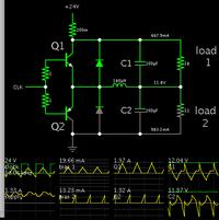
I wonder if this simulation is close what you had in mind? The inductor is placed where it serves a dual role, for an upper and lower buck converter.


The presence of the inductor stops the sudden current surges which are characteristic with capacitors.

Less Amperes are drawn from the 24V supply.

A benefit is that the midway node maintains a reasonably stable volt level. One of the loads is lighter than the other in my simulation, yet they receive approximately the same voltage.

The clock is 50% duty cycle. It alternately turns the transistors on and off. However there may be times when only one transistor needs to be turned on, to give a supplemental charge to one capacitor. Then it can be turned off.

Therefore an improvement might be a dual clock, or a tri-state device.
 

Status
Not open for further replies.

Similar threads

Part and Inventory Search

Welcome to EDABoard.com

Sponsor

Back
Top