Continue to Site

Welcome to EDAboard.com

Welcome to our site! EDAboard.com is an international Electronics Discussion Forum focused on EDA software, circuits, schematics, books, theory, papers, asic, pld, 8051, DSP, Network, RF, Analog Design, PCB, Service Manuals... and a whole lot more! To participate you need to register. Registration is free. Click here to register now.

Keyfob(CC2541 Mini-DK) PCB layout design in PADS 9.xx

Status
Not open for further replies.

sarang1993

Newbie level 2
Joined
Dec 25, 2014
Messages
2
Helped
0
Reputation
0
Reaction score
0
Trophy points
1
Activity points
14
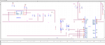
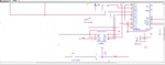
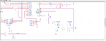
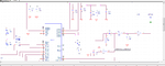
We are making keyfob with some modifications we have been told to use PADS software im trying to design the layout but not getting it right, what are the rules for designinig keyfob, like how much distance(in mils) between capacitors,resistors,RF section also where to place decoupling capacitors and arrangemennt of other components, trace/track width can anyone give me reference design so it would be helpful. I have also attached the schematic images we have made in OrCAD 16.3 so anyone would suggest me???
if anyone wants to see my schematic just post ur e-mail id
 

Attachments

  • 1.png
    1.png
    55.9 KB · Views: 94
  • 2.png
    2.png
    52.8 KB · Views: 88
  • 3.png
    3.png
    53.4 KB · Views: 95
  • 4.png
    4.png
    59.7 KB · Views: 89
  • 5.png
    5.png
    43.2 KB · Views: 95

Status
Not open for further replies.

Part and Inventory Search

Welcome to EDABoard.com

Sponsor

Back
Top