Continue to Site

Welcome to EDAboard.com

Welcome to our site! EDAboard.com is an international Electronics Discussion Forum focused on EDA software, circuits, schematics, books, theory, papers, asic, pld, 8051, DSP, Network, RF, Analog Design, PCB, Service Manuals... and a whole lot more! To participate you need to register. Registration is free. Click here to register now.

Nexys 3 Board problem with reading /writing registers

Status
Not open for further replies.

makanaky

Advanced Member level 4
Joined
Feb 1, 2007
Messages
104
Helped
0
Reputation
0
Reaction score
0
Trophy points
1,296
Activity points
1,944
Hi,

I wrote a software that writes data to the FPGA register, and read the processing results. I found that for repetitive read/write, the software fails to read registers anymore (the DpcPutReg function returns -1)
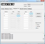
I also tried to make this using Adept software, after some (10~30) reads/writes, I cannot read/write registers anymore and I need to reprogram the bit file as attached. Can you please support me with this or tell me what's wrong ?

Thanks
 

My mind reading skills aren't what they used to be.
Post your complete code please.
 

My mind reading skills aren't what they used to be.
Post your complete code please.

Hi Shaiko :

Here's my cpp code : It basically reads a file (Read.txt) of integers ranging from -7 to 7 , input these to the FPGA which processes these values, and registers '1' in case of positive value, '0' otherwise. The software then writes theses comparator results to another file (Write.txt). The operation is successfu for the 1st few values only, after that values of -1 only are written in the output file which means that the register cannot be read. Also reading using Digilent software fails

Code:
#include <windows.h>
#include <stdio.h>
#include <iostream>
#include <stdlib.h>
#include <string.h>
#include "dpcdefs.h"
#include "dpcutil.h"
#include "dpcdecl.h"
#include "dmgr.h"

#include <iostream>
#include <fstream>
#include <string>

using namespace std;
char device[17];
static int PutReg(unsigned char r, unsigned char *b, int len) {

	ERC		erc;
	HANDLE	hif;

	if (!DpcOpenData(&hif, device, &erc, NULL)) {
		goto fail;
	}

	if(len == 1)
	{
		if(!DpcPutReg(hif, r, *b, &erc, NULL)) {
			DpcCloseData(hif,&erc);
			goto fail;
		}
	}
	else
	{
		if(!DpcPutRegRepeat(hif, r, b, len, &erc, NULL)) {
			DpcCloseData(hif,&erc);
			goto fail;
		}
	}

	erc = DpcGetFirstError(hif);
	DpcCloseData(hif, &erc);

	if (erc == ercNoError) 
		return 0;

fail:
	return -1;
}
 
static int GetReg(unsigned char r) {

	unsigned char b;
	ERC		erc;
	HANDLE	hif;

	if (!DpcOpenData(&hif, device, &erc, NULL)) {
		goto fail;
	}

	if (!DpcGetReg(hif, r, &b, &erc, NULL)) {
		DpcCloseData(hif,&erc);
		goto fail;
	}

	erc = DpcGetFirstError(hif);
	DpcCloseData(hif, &erc);

	if (erc == ercNoError) 
		return b;
fail: 
	return -1;
}

int main()

{
  string line_read,line_wr;
  ifstream myfile_rd ("Read.txt");
  ofstream myfile_wr ("write.txt");	 

HANDLE * phif1 = 0 ;
ERC * perc1 = ercNoError;
int f =0 ;
TRID * ptrid1 = 0;
BOOL x,y;
x= DpcInit(&f);
int x1 =0 ;
int x2 = 0 ;
char * y1;


/*
//Configure device, Get connected devices, give alias to use to 
//handle communications with the device
HWND x3=0;
DvmgStartConfigureDevices( x3, &x2);*/


int id,erc=0;
//Get device ID
id = DvmgGetDefaultDev(&erc);
//Get device name 
DvmgGetDevName(id, device, &erc);
//print device name 
printf("Your FPGA device is aliased : %s \n",device);
//Register write
int read_input;
  if (myfile_rd.is_open())
  {
    while ( getline (myfile_rd,line_read) )
    {
		read_input=atoi(line_read.c_str());


	unsigned char *a;
	unsigned char b;

	//b=(unsigned char)(aa);
	//printf(" b value : %d \n",b);
	unsigned char hh=(unsigned char)read_input;
	a=&hh;
	//printf("%c",*a);
	PutReg(char(0),a,1);
	//Sleep(100);
//Register read
	int value,reg_rd_id;
	reg_rd_id = 11;
	value = GetReg(reg_rd_id);
	Sleep(5000);
	//line_wr = static_cast<ostringstream*>( &(ostringstream() << value) )->str();
    myfile_wr << value << '\n' ;
    }
    myfile_rd.close();
    myfile_wr.close();
  }

  else cout << "Unable to open file"; 
  printf("Finished Processing ! \n");
cin.get();

return 0;
}
 

Attachments

  • Capture1.JPG
    Capture1.JPG
    76.9 KB · Views: 73

Where is your HDL design file?
 

This is the top level :

Code:
----------------------------------------------------------------------------
--	dig_equalizer.VHD -- Digilent Parallel Interface Module Reference Design
----------------------------------------------------------------------------
-- Author:  Gene Apperson
--          Copyright 2004 Digilent, Inc.
----------------------------------------------------------------------------
-- IMPORTANT NOTE ABOUT BUILDING THIS LOGIC IN ISE
--
-- Before building the dig_equalizer logic in ISE:
-- 	1.  	In Project Navigator, right-click on "Synthesize-XST"
--		(in the Process View Tab) and select "Properties"
--	2.	Click the "HDL Options" tab
--	3. 	Set the "FSM Encoding Algorithm" to "None"
----------------------------------------------------------------------------
--
----------------------------------------------------------------------------
--	This module contains an example implementation of Digilent Parallel
--	Interface Module logic. This interface is used in conjunction with the
--	DPCUTIL DLL and a Digilent Communications Module (USB, EtherNet, Serial)
--	to exchange data with an application running on a host PC and the logic
--	implemented in a gate array.
--
--	See the Digilent document, Digilent Parallel Interface Model Reference
--	Manual (doc # 560-000) for a description of the interface.
--
--	This design uses a state machine implementation to respond to transfer
--	cycles. It implements an address register, 8 internal data registers
--	that merely hold a value written, and interface registers to communicate
--	with a Digilent DIO4 board. There is an LED output register whose value 
--	drives the 8 discrete leds on the DIO4. There are two input registers.
--	One reads the switches on the DIO4 and the other reads the buttons.
--
--	Interface signals used in top level entity port:
--		mclk		- master clock, generally 50Mhz osc on system board
--		pdb			- port data bus
--		astb		- address strobe
--		dstb		- data strobe
--		pwr			- data direction (described in reference manual as WRITE)
--		pwait		- transfer synchronization (described in reference manual
--						as WAIT)
--		rgLed		- LED outputs to the DIO4
--		rgSwt		- switch inputs from the DIO4
--		ldb			- led gate signal for the DIO4
--		rgBtn		- button inputs from the DIO4
--		btn			- button on system board (D2SB or D2FT)
--		led			- led on the system board
--		
----------------------------------------------------------------------------
-- Revision History:
--  06/09/2004(GeneA): created
--	08/10/2004(GeneA): initial public release
--	04/25/2006(JoshP): comment addition  
----------------------------------------------------------------------------

library IEEE;
use IEEE.STD_LOGIC_1164.ALL;
use IEEE.NUMERIC_STD.ALL;
--use IEEE.STD_LOGIC_ARITH.ALL;
--use IEEE.STD_LOGIC_UNSIGNED.ALL;

--  Uncomment the following lines to use the declarations that are
--  provided for instantiating Xilinx primitive components.
--library UNISIM;
--use UNISIM.VComponents.all;

entity dig_equalizer is
    Port (
	   reset : in std_logic;
		mclk 	: in std_logic;
        pdb		: inout std_logic_vector(7 downto 0);
        astb 	: in std_logic;
        dstb 	: in std_logic;
        pwr 	: in std_logic;
        pwait 	: out std_logic;
		rgLed	: out std_logic_vector(7 downto 0); 
		rgSwt	: in std_logic_vector(7 downto 0);
		rgBtn	: in std_logic_vector(4 downto 0);
		btn		: in std_logic;
		ldg		: out std_logic;
		led		: out std_logic
	);
end dig_equalizer;

architecture Behavioral of dig_equalizer is

------------------------------------------------------------------------
-- Component Declarations
------------------------------------------------------------------------

------------------------------------------------------------------------
-- Local Type Declarations
------------------------------------------------------------------------

------------------------------------------------------------------------
--  Constant Declarations
------------------------------------------------------------------------

	-- The following constants define state codes for the EPP port interface
	-- state machine. The high order bits of the state number give a unique
	-- state identifier. The low order bits are the state machine outputs for
	-- that state. This type of state machine implementation uses no
	-- combination logic to generate outputs which should produce glitch
	-- free outputs.
	constant	stEppReady	: std_logic_vector(7 downto 0) := "0000" & "0000";
	constant	stEppAwrA	: std_logic_vector(7 downto 0) := "0001" & "0100";
	constant	stEppAwrB	: std_logic_vector(7 downto 0) := "0010" & "0001";
	constant	stEppArdA	: std_logic_vector(7 downto 0) := "0011" & "0010";
	constant	stEppArdB	: std_logic_vector(7 downto 0) := "0100" & "0011";
	constant	stEppDwrA	: std_logic_vector(7 downto 0) := "0101" & "1000";
	constant	stEppDwrB	: std_logic_vector(7 downto 0) := "0110" & "0001";
	constant	stEppDrdA	: std_logic_vector(7 downto 0) := "0111" & "0010";
	constant	stEppDrdB	: std_logic_vector(7 downto 0) := "1000" & "0011";

------------------------------------------------------------------------
-- Signal Declarations
------------------------------------------------------------------------

	-- State machine current state register
	signal	stEppCur	: std_logic_vector(7 downto 0) := stEppReady;

	signal	stEppNext	: std_logic_vector(7 downto 0);

	signal	clkMain		: std_logic;

	-- Internal control signales
	signal	ctlEppWait	: std_logic;
	signal	ctlEppAstb	: std_logic;
	signal	ctlEppDstb	: std_logic;
	signal	ctlEppDir	: std_logic;
	signal	ctlEppWr	: std_logic;
	signal	ctlEppAwr	: std_logic;
	signal	ctlEppDwr	: std_logic;
	signal	busEppOut	: std_logic_vector(7 downto 0);
	signal	busEppIn	: std_logic_vector(7 downto 0);
	signal	busEppData	: std_logic_vector(7 downto 0);

	-- Registers
	signal	regEppAdr	: std_logic_vector(3 downto 0);
	signal	regData0	: std_logic_vector(7 downto 0);
	signal	regData1	: std_logic_vector(7 downto 0);
    signal  regData2	: std_logic_vector(7 downto 0);
    signal  regData3	: std_logic_vector(7 downto 0);
    signal  regData4	: std_logic_vector(7 downto 0);
	signal	regData5	: std_logic_vector(7 downto 0);
	signal	regData6	: std_logic_vector(7 downto 0);
	signal	regData7	: std_logic_vector(7 downto 0);
	signal	regLed		: std_logic_vector(7 downto 0);
   signal cntr_100 : unsigned(31 downto 0);
	signal div100 : std_logic;
	signal	cntr		: unsigned(23 downto 0); 
   signal clk_div100 : std_logic;
	signal reg_result_0,reg_result_1 : std_logic_vector(7 downto 0);
	signal Result_mul : std_logic_vector(15 downto 0);
	signal outdata_s : std_logic;
------------------------------------------------------------------------
-- Component Declaration
------------------------------------------------------------------------	

Component limiter is
    Port ( clk : in  STD_LOGIC;
           reset : in  STD_LOGIC;
           in_data : in  STD_LOGIC_VECTOR (3 downto 0);
           out_data : out  STD_LOGIC);
end Component;
------------------------------------------------------------------------
-- Module Implementation
------------------------------------------------------------------------

begin

    ------------------------------------------------------------------------
	-- Map basic status and control signals
    ------------------------------------------------------------------------
process(reset,mclk) is
begin
if reset='1' then
cntr_100 <= x"00000000";
div100<='0';
elsif rising_edge(mclk) then
if (cntr_100=x"05F5E100") then
cntr_100 <= x"00000000";
div100<=not(div100);
else
cntr_100 <= cntr_100+1;
end if;
end if;
end process;

limiter_0 : limiter 
    port map( clk => mclk,
           reset => reset,
           in_data => regData0(3 downto 0),
           out_data => outdata_s);


	  process (mclk,reset) is
	  begin
	  if reset='1' then
		reg_result_0 <= (others=>'0');	
	  elsif rising_edge(mclk) then
		reg_result_0 <= "0000000" & outdata_s;
	  end if;
	  end process;

	clkMain <= mclk;

	ctlEppAstb <= astb;
	ctlEppDstb <= dstb;
	ctlEppWr   <= pwr;
	pwait      <= ctlEppWait;	-- drive WAIT from state machine output

	-- Data bus direction control. The internal input data bus always
	-- gets the port data bus. The port data bus drives the internal
	-- output data bus onto the pins when the interface says we are doing
	-- a read cycle and we are in one of the read cycles states in the
	-- state machine.
	busEppIn <= pdb;
	pdb <= busEppOut when ctlEppWr = '1' and ctlEppDir = '1' else "ZZZZZZZZ";

	-- Select either address or data onto the internal output data bus.
	busEppOut <= "0000" & regEppAdr when ctlEppAstb = '0' else busEppData;

	rgLed <= Result_mul(7 downto 0);
	ldg <= '1';

	-- Decode the address register and select the appropriate data register
	busEppData <=	regData0 when regEppAdr = "0000" else
					regData1 when regEppAdr = "0001" else
					regData2 when regEppAdr = "0010" else
					regData3 when regEppAdr = "0011" else
					regData4 when regEppAdr = "0100" else
					regData5 when regEppAdr = "0101" else
					regData6 when regEppAdr = "0110" else
					regData7 when regEppAdr = "0111" else
					rgSwt    when regEppAdr = "1000" else
					"000" & rgBtn when regEppAdr = "1001" else
					"10011001" when regEppAdr = "1010" else
					reg_result_0 when regEppAdr = "1011" else
					reg_result_1 when regEppAdr = "1100" else
						"00000000";

    ------------------------------------------------------------------------
	-- EPP Interface Control State Machine
    ------------------------------------------------------------------------

	-- Map control signals from the current state
	ctlEppWait <= stEppCur(0);
	ctlEppDir  <= stEppCur(1);
	ctlEppAwr  <= stEppCur(2);
	ctlEppDwr  <= stEppCur(3);

	-- This process moves the state machine to the next state
	-- on each clock cycle
	process (clkMain)
		begin
			if clkMain = '1' and clkMain'Event then
				stEppCur <= stEppNext;
			end if;
		end process;

	-- This process determines the next state machine state based
	-- on the current state and the state machine inputs.
	process (stEppCur, stEppNext, ctlEppAstb, ctlEppDstb, ctlEppWr)
		begin
			case stEppCur is
				-- Idle state waiting for the beginning of an EPP cycle
				when stEppReady =>
					if ctlEppAstb = '0' then
						-- Address read or write cycle
						if ctlEppWr = '0' then
							stEppNext <= stEppAwrA;
						else
							stEppNext <= stEppArdA;
						end if;

					elsif ctlEppDstb = '0' then
						-- Data read or write cycle
						if ctlEppWr = '0' then
							stEppNext <= stEppDwrA;
						else
							stEppNext <= stEppDrdA;
						end if;

					else
						-- Remain in ready state
						stEppNext <= stEppReady;
					end if;											

				-- Write address register
				when stEppAwrA =>
					stEppNext <= stEppAwrB;

				when stEppAwrB =>
					if ctlEppAstb = '0' then
						stEppNext <= stEppAwrB;
					else
						stEppNext <= stEppReady;
					end if;		

				-- Read address register
				when stEppArdA =>
					stEppNext <= stEppArdB;

				when stEppArdB =>
					if ctlEppAstb = '0' then
						stEppNext <= stEppArdB;
					else
						stEppNext <= stEppReady;
					end if;

				-- Write data register
				when stEppDwrA =>
					stEppNext <= stEppDwrB;

				when stEppDwrB =>
					if ctlEppDstb = '0' then
						stEppNext <= stEppDwrB;
					else
 						stEppNext <= stEppReady;
					end if;

				-- Read data register
				when stEppDrdA =>
					stEppNext <= stEppDrdB;
										
				when stEppDrdB =>
					if ctlEppDstb = '0' then
						stEppNext <= stEppDrdB;
					else
				  		stEppNext <= stEppReady;
					end if;

				-- Some unknown state				
				when others =>
					stEppNext <= stEppReady;

			end case;
		end process;
		
    ------------------------------------------------------------------------
	-- EPP Address register
    ------------------------------------------------------------------------

	process (clkMain, ctlEppAwr)
		begin
			if clkMain = '1' and clkMain'Event then
				if ctlEppAwr = '1' then
					regEppAdr <= busEppIn(3 downto 0);
				end if;
			end if;
		end process;

    ------------------------------------------------------------------------
	-- EPP Data registers
    ------------------------------------------------------------------------
 	-- The following processes implement the interface registers. These
	-- registers just hold the value written so that it can be read back.
	-- In a real design, the contents of these registers would drive additional
	-- logic.
	-- The ctlEppDwr signal is an output from the state machine that says
	-- we are in a 'write data register' state. This is combined with the
	-- address in the address register to determine which register to write.

	process (clkMain, regEppAdr, ctlEppDwr, busEppIn)
		begin
			if clkMain = '1' and clkMain'Event then
				if ctlEppDwr = '1' and regEppAdr = "0000" then
					regData0 <= busEppIn;
				end if;
			end if;
		end process;

	process (clkMain, regEppAdr, ctlEppDwr, busEppIn)
		begin
			if clkMain = '1' and clkMain'Event then
				if ctlEppDwr = '1' and regEppAdr = "0001" then
					regData1 <= busEppIn;
				end if;
			end if;
		end process;

	process (clkMain, regEppAdr, ctlEppDwr, busEppIn)
		begin
			if clkMain = '1' and clkMain'Event then
				if ctlEppDwr = '1' and regEppAdr = "0010" then
					regData2 <= busEppIn;
				end if;
			end if;
		end process;

	process (clkMain, regEppAdr, ctlEppDwr, busEppIn)
		begin
			if clkMain = '1' and clkMain'Event then
				if ctlEppDwr = '1' and regEppAdr = "0011" then
					regData3 <= busEppIn;
				end if;
			end if;
		end process;

	process (clkMain, regEppAdr, ctlEppDwr, busEppIn)
		begin
			if clkMain = '1' and clkMain'Event then
				if ctlEppDwr = '1' and regEppAdr = "0100" then
					regData4 <= busEppIn;
				end if;
			end if;
		end process;

	process (clkMain, regEppAdr, ctlEppDwr, busEppIn)
		begin
			if clkMain = '1' and clkMain'Event then
				if ctlEppDwr = '1' and regEppAdr = "0101" then
					regData5 <= busEppIn;
				end if;
			end if;
		end process;

	process (clkMain, regEppAdr, ctlEppDwr, busEppIn)
		begin
			if clkMain = '1' and clkMain'Event then
				if ctlEppDwr = '1' and regEppAdr = "0110" then
					regData6 <= busEppIn;
				end if;
			end if;
		end process;

	process (clkMain, regEppAdr, ctlEppDwr, busEppIn)
		begin
			if clkMain = '1' and clkMain'Event then
				if ctlEppDwr = '1' and regEppAdr = "0111" then
					regData7 <= busEppIn;
				end if;
			end if;
		end process;

	process (clkMain, regEppAdr, ctlEppDwr, busEppIn)
		begin
			if clkMain = '1' and clkMain'Event then
				if ctlEppDwr = '1' and regEppAdr = "1010" then
					regLed <= busEppIn;
				end if;
			end if;
		end process;


	------------------------------------------------------------------------
    -- Gate array configuration verification logic
	------------------------------------------------------------------------
	-- This logic will flash the led on the gate array. This is to verify
	-- that the gate array is properly configured for the test. This is a
	-- simple way to verify that the gate array actually got configured.

 	led <= btn or cntr(23);

	process (clkMain)
		begin
			if clkMain = '1' and clkMain'Event then
				cntr <= cntr + 1;
			end if;
		end process;

----------------------------------------------------------------------------

end Behavioral;

This is the limiter component :

Code:
----------------------------------------------------------------------------------
-- Company: 
-- Engineer: 
-- 
-- Create Date:    23:25:19 09/19/2014 
-- Design Name: 
-- Module Name:    limiter - Behavioral 
-- Project Name: 
-- Target Devices: 
-- Tool versions: 
-- Description: 
--
-- Dependencies: 
--
-- Revision: 
-- Revision 0.01 - File Created
-- Additional Comments: 
--
----------------------------------------------------------------------------------
library IEEE;
use IEEE.STD_LOGIC_1164.ALL;

-- Uncomment the following library declaration if using
-- arithmetic functions with Signed or Unsigned values
use IEEE.NUMERIC_STD.ALL;

-- Uncomment the following library declaration if instantiating
-- any Xilinx primitives in this code.
--library UNISIM;
--use UNISIM.VComponents.all;

entity limiter is
    Port ( clk : in  STD_LOGIC;
           reset : in  STD_LOGIC;
           in_data : in  STD_LOGIC_VECTOR (3 downto 0);
           out_data : out  STD_LOGIC);
end limiter;

architecture Behavioral of limiter is

begin

process(clk,reset) is
begin
if(reset='1') then
	out_data <= '0';
elsif(rising_edge(clk)) then
	out_data <= not(in_data(3));
end if;
end process;

end Behavioral;
 

Did you try to simulate it yourself?
 

I meant the whole design. Not just the limiter component.
 

I meant the whole design. Not just the limiter component.

Yea I know, its just registers read/write . plus this is the template provided by digilent anyway and its not a functional bug , its a hardware issue that the register cannot be read/written
 

Status
Not open for further replies.

Part and Inventory Search

Welcome to EDABoard.com

Sponsor

Back
Top