Welcome to our site! EDAboard.com is an international Electronics Discussion Forum focused on EDA software, circuits, schematics, books, theory, papers, asic, pld, 8051, DSP, Network, RF, Analog Design, PCB, Service Manuals... and a whole lot more! To participate you need to register. Registration is free. Click here to register now.
I am new to Analog IC design. Could some one please help me with derivation of biasing circuits for a complementary differential pair input for a rail to rail operational amplifier. (Please see the attached .jpg for reference )
Could I get a reference as to how the bias generator works( for example the one you have attached ) i.e. the principle of operation; so that when I would need to derive a particular bias circuit, I could do it myself with more of intuitive understanding
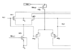
I've found this circuit some time ago in this very forum, but don't remember when. Perhaps you can retrace it. Here its operation in short form:
The first two vertical branches represent a bias current generator (with positive feedback < 1).
The current value is given by the W/L ratio, the resistor and the VCC values.
The upmost left PMOS generates the positive bias voltage VBP which also supplies the 2 following vertical branches.
Via VBP the bias current is mirrored to the 3rd vertical branch, which generates via its NMOS in diode connection the negative bias voltage VBN.
The cascode PMOSes and NMOS, together with the 2 bottom-most NMOSes are operated as switches and can enable/disable the current flow. If disabled (EN_bar=1, EN=0), VBN=VBP=VSS.
It should be verified if VBP=VSS in the disabled state is appropriate for the following circuit.
This site uses cookies to help personalise content, tailor your experience and to keep you logged in if you register.
By continuing to use this site, you are consenting to our use of cookies.