Continue to Site

Welcome to EDAboard.com

Welcome to our site! EDAboard.com is an international Electronics Discussion Forum focused on EDA software, circuits, schematics, books, theory, papers, asic, pld, 8051, DSP, Network, RF, Analog Design, PCB, Service Manuals... and a whole lot more! To participate you need to register. Registration is free. Click here to register now.

Questions about colpitts oscillator design?

Status
Not open for further replies.
Hi samy,

I suppose you are aware that you make use of the configuration in Fig. 2.18-A .
 

RE(total) = RE + re = 1500+26 = 1526 ohm
RB = R2//R4//(beta*[re+RE])= 14.5 kohm.
Some points why the calculation isn't right.
- output impedance of common collector circuit (for shorted input), you call it RE(total), is RE || re ≈ re
- beta at 148 MHz isn't equal betaDC. According to fT of 300 MHz, it's only about 2. The problem has been addressed in post #7.
- amplifier input and output impedance, load and source resistance are strongly mutually dependent in the CC circuit. That's a reason, why "impedance matching" doesn't achieve results representative for the circuit operation. Analyzing the circuit as CB with virtual ground, as suggested by LvW, gives a better decoupling of both amplifier ports.

Impedance matching isn't a bad design idea, when the amplifier power gain is small and must be well utilized to get the oscillator working at all. But it must consider the actual frequency dependent transistor parameters.

At frequencies with a sufficient gain margin, impedance matching isn't the right concept to design an oscillator feedback path.
 

Hi samy,

I suppose you are aware that you make use of the configuration in Fig. 2.18-A .

yes I Know, thanks

- - - Updated - - -

Some points why the calculation isn't right.
- output impedance of common collector circuit (for shorted input), you call it RE(total), is RE || re ≈ re
Yes, you're right

- beta at 148 MHz isn't equal betaDC. According to fT of 300 MHz, it's only about 2. The problem has been addressed in post #7.
Yes, you're right. Although I read # 7 and well-screened, but I rushed when I saw the book.

- amplifier input and output impedance, load and source resistance are strongly mutually dependent in the CC circuit. That's a reason, why "impedance matching" doesn't achieve results representative for the circuit operation. Analyzing the circuit as CB with virtual ground, as suggested by LvW, gives a better decoupling of both amplifier ports.
I frankly do not understand very well what LvW tried to say, if necessary I hope larger and step by step
explain I will try it.

Impedance matching isn't a bad design idea, when the amplifier power gain is small and must be well utilized to get the oscillator working at all. But it must consider the actual frequency dependent transistor parameters.

At frequencies with a sufficient gain margin, impedance matching isn't the right concept to design an oscillator feedback path.
Yes
On the whole, I feel very frustrated, but I'm going to resist

I guess there's certainly a not complicated solution
I will leave the next step to you
Thank you for your cooperation
 

I guess there's certainly a not complicated solution
I will leave the next step to you

As you said, you're tired of books and articles.

Formulas can only take us so far.

Of course the reality came first. Later came the math.

As for the concepts of operation, these are not so easy to grasp.

Simulations have become extremely useful in this area.

For an aid to understanding the operation of these LC tank oscillators, I suggest you watch my Youtube videos which show an animation of Colpitts and Clapp oscillators.

It graphically portrays current flowing through wires.
Also changing coil flux and emf.
Also capacitors charging and discharging.

Colpitts type:

https://youtu.be/mnlIifVnHSU

Clapp type (You will find your configuration resembles the last half of the video):

https://youtu.be/wKnarrvynIw
 

Some points why the calculation isn't right.
- output impedance of common collector circuit (for shorted input), you call it RE(total), is RE || re ≈ re

It's a pity that samy uses symbols without sufficient explanation, but I think he didn't make any error as far as RE is concerned (but I am surprised about his comment "yes, you are right").
According to his calculation I suppose the symbol "RB" stands for the resulting DYNAMIC input resistance of the whole amplifier stage and the symbol "RE(total)=RE+re" is just an intermediate step for the sum of two resistances.
After multiplication of this "fictive" value RE(total) with beta we arrive at the DYNAMIC input resistance looking into the base r_base.

Thus, with h21=beta and h11=common emitter short circuit input resistance we get:

r_base=h11 + h21*RE = h21*(h11/h21 + RE)=h21*(re+RE) with re=1/g=internal emitter resistance and g=transconductance.

Remark: This calculation did not yet consider the frequency-selective feedback path connected to the emitter as well as the load resistor (500 ohms).

Recommendation to samy:
1.) Please explain all calculations and symbols in order to avoid misunderstandings (wasting of time).
2.) Distinguish between static/ohmic resistors (large symbols R) and dynamic resistances (small symbols r).

- - - Updated - - -

I frankly do not understand very well what LvW tried to say, if necessary I hope larger and step by step
explain I will try it.

Supplementing my explanations in post#17 I should mention that in CC configuration also the collector node must be considered as dynamically (ac) grounded.
(That means: Also this node has to be released from ground potential for transforming the CC in an equivalent CB configuration)
 
Last edited:

As you said, you're tired of books and articles.

Formulas can only take us so far.

Of course the reality came first. Later came the math.

As for the concepts of operation, these are not so easy to grasp.

Simulations have become extremely useful in this area.
First, thank you for Videos
The most beautiful I heard your voice
Now: The last words I have to say here I am convinced that the design is done by simulation.
Thank you all
You gave everything you can to help me
I appreciate it

- - - Updated - - -

Recommendation to samy:
1.) Please explain all calculations and symbols in order to avoid misunderstandings (wasting of time).
2.) Distinguish between static/ohmic resistors (large symbols R) and dynamic resistances (small symbols r).
I will do my best in the following discussions that take these tips into consideration
Thank you for your help
 

I'm somewhat surprized, that the circuit under discussion has been repeatedly associated with the clapp oscillator topology.
It's true, that the original circuit also covers the clapp oscillator option by making C0 small and constituating a series LC resonantor. But it has been clarified from the start that C0 is sufficient large to act as a DC block only.

Functionally, series resonant clapp and parallel resonant colpitts circuit are sufficiently different to distinguish them in the discussion. The exact analysis of the colpitts circuit is already demanding enough.

Yes, the capacitor next to the coil is large compared to the other 2 caps. It has little influence on the tank resonant frequency.

However it must charge up initially before oscillations get underway. Since it is a large uF value, this takes substantial time. The circuit can easily stagnate. It is not guaranteed to start oscillating.

So it should probably be reduced. Perhaps to the point where it will influence resonant frequency.

I'm somewhat surprized, that the circuit under discussion has been repeatedly associated with the clapp oscillator topology.

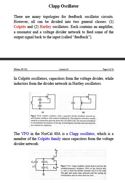
The Clapp type is in the Colpitts family.

I am acquainted with this oscillator. It is discussed in articles about the NorCal radio transceiver. (A well-designed unit which became popular due to its reliability and functionality.)

The screenshot below is from an article about the oscillator used. It calls it a Clapp type, a cousin of the Colpitts.

Subsequent pages show math calculations. I see a formula for resonant frequency. It includes all three capacitors. This implies the one next to the inductor is small enough to have an influence along with the other capacitors.

**broken link removed**

- - - Updated - - -

69_1346625682.png
 

I agree to the visual presentation of the clapp and colpitts relation. A C0 value of 1 nF as chosen in the begin of this thread is apart from having noticeable influence on the oscillation frequency but doesn't cause problems in simulation.

In the real circuit, a large coupling capacitor won't prevent oscillation, it's a pure simulation issue (as long as we consider linear oscillators).
 

Status
Not open for further replies.

Similar threads

Part and Inventory Search

Welcome to EDABoard.com

Sponsor

Back
Top