ishailesh
Junior Member level 3
- Joined
- Apr 4, 2012
- Messages
- 31
- Helped
- 6
- Reputation
- 12
- Reaction score
- 6
- Trophy points
- 1,288
- Location
- New Delhi, India
- Activity points
- 1,652
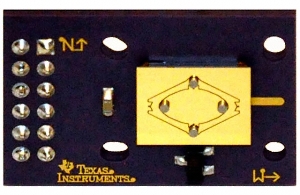
I am working on pcb layout. In that i have to generate a footprint for TALP1000 b analog pointing mirror.
As of now i am unable to get pin size and other relevant mechanical specification. I have browse through its datasheet but they are not providing the pin sizes. So any help in this problem would be appreciated.Thanks
Regards
As of now i am unable to get pin size and other relevant mechanical specification. I have browse through its datasheet but they are not providing the pin sizes. So any help in this problem would be appreciated.Thanks
Regards