Continue to Site

Welcome to EDAboard.com

Welcome to our site! EDAboard.com is an international Electronics Discussion Forum focused on EDA software, circuits, schematics, books, theory, papers, asic, pld, 8051, DSP, Network, RF, Analog Design, PCB, Service Manuals... and a whole lot more! To participate you need to register. Registration is free. Click here to register now.

Provision for faster discharge of the gate of a MOSFET

Status
Not open for further replies.

gdylp2004

Member level 5
Joined
Dec 4, 2011
Messages
81
Helped
0
Reputation
0
Reaction score
0
Trophy points
1,286
Activity points
2,192
Hi guys,

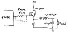
As seen in the attached schematic, the PWM controls the nMOS by charging and discharging the gate accordingly. While running the buck for a min or two, the MOSFET's TO-220 package temperature rised to about >160 °C and I've burnt 2 nMOS before (note that the max. absolute temperature rating for the IRF640N is 150 °C).

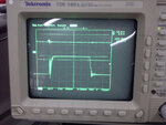
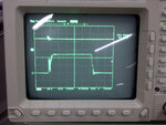
To tackle the prob, I've added a diode anti-parallel with Rgate to provide an alternate path for the gate to discharge upon turning off. However, when I observed my o-scope under the 2 conditions (with and w/o diode), there seems no significant change is the dv/dt of the gate-source voltage. It remains at about 350ns.

Do anyone know why? Could it be the diode's intrisic resistance is also close to 5.6Ω as well?

The diode I used is MUR120 Ultra-fast recovery diode.
 

Attachments

  • with_diode.jpg
    with_diode.jpg
    105.4 KB · Views: 53
  • without_diode.jpg
    without_diode.jpg
    109.7 KB · Views: 54
  • paint_buck.jpg
    paint_buck.jpg
    40.4 KB · Views: 61

Is the gate waveform to scale? It looks like its amplitude is only 250mV.

What does the rest of the gate drive circuit look like? Are you using a gate driver IC?
 

Is the gate waveform to scale? It looks like its amplitude is only 250mV.

What does the rest of the gate drive circuit look like? Are you using a gate driver IC?

I am using a diff. probe with a 100mV/div translate into 5V/div scaling factor. Yes, I'm using a IR2117 gate driver with all my details in this thread: https://www.edaboard.com/threads/233047/.
 

Okay, if it's that slow then parasitic inductance on your gate drive leads (and the rest of the converter in general) is probably the main cause. Make them as short as possible (like a few inches at most), and use twisted pairs to reduce inductance. Shrinking the area of the loop formed by the input bypass capacitor, MOSFET, and catch diode will also reduce stay inductance and reduce ringing. That should help significantly. But if you want switching times of 100ns or less you'll probably need a tighter layout than that, with everything on the same board.
 
Okay, if it's that slow then parasitic inductance on your gate drive leads (and the rest of the converter in general) is probably the main cause. Make them as short as possible (like a few inches at most), and use twisted pairs to reduce inductance. Shrinking the area of the loop formed by the input bypass capacitor, MOSFET, and catch diode will also reduce stay inductance and reduce ringing. That should help significantly. But if you want switching times of 100ns or less you'll probably need a tighter layout than that, with everything on the same board.
Right, I'm already planning to put all on a board. Will post some results when ready.

Thanks for your advice.
 

Status
Not open for further replies.

Part and Inventory Search

Welcome to EDABoard.com

Sponsor

Back
Top