ffsher100
Junior Member level 3
Hi all,
I am new to analog world and survey some opamp's simulation document for a while.
I got question about "open loop gain"
While open_loop_gain state, my understand is that all mos in opamp should be satisfied with Saturation.
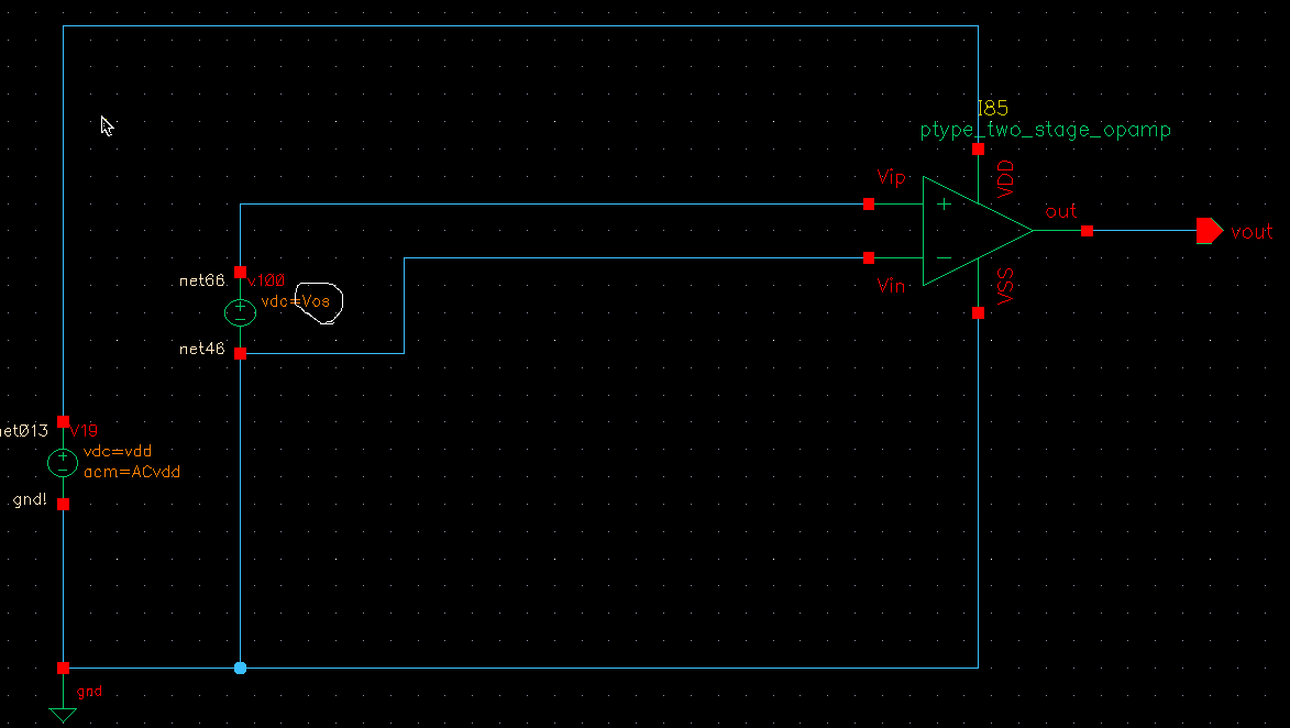
first, i use dc sweep offset voltage between inverter(vip) non-inverter(vin)
vip more than vin
Thus, i put Vos(offset voltage) -1.4mv on vip such that vin=vdd/2, vip=(vdd/2)-1.4mv and all mos in saturation.
.TF V(vout) vip also let me obtain open loop gain in hspice report.
is this right way to find open loop gain??
I am new to analog world and survey some opamp's simulation document for a while.
I got question about "open loop gain"
While open_loop_gain state, my understand is that all mos in opamp should be satisfied with Saturation.
first, i use dc sweep offset voltage between inverter(vip) non-inverter(vin)
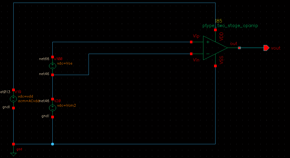
vip more than vin
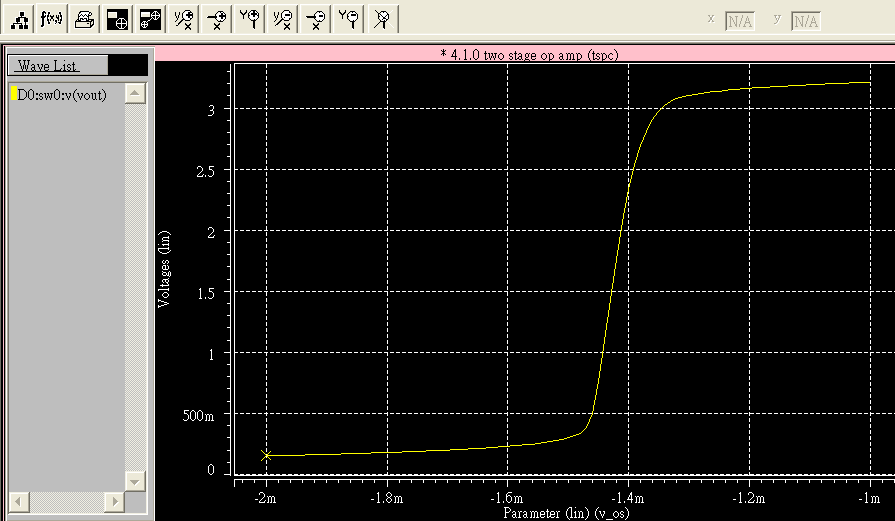
Thus, i put Vos(offset voltage) -1.4mv on vip such that vin=vdd/2, vip=(vdd/2)-1.4mv and all mos in saturation.
.TF V(vout) vip also let me obtain open loop gain in hspice report.
is this right way to find open loop gain??
Last edited:
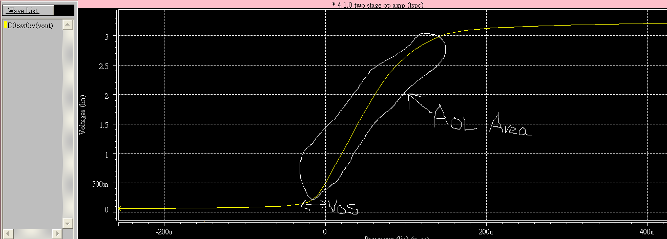
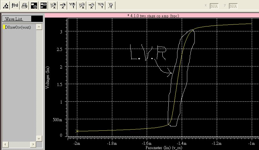
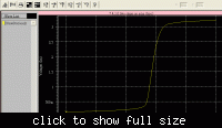
 1.65v-2mv)~(1.65v+1mv) while vin(invert) keep 1.65v.