Continue to Site

Welcome to EDAboard.com

Welcome to our site! EDAboard.com is an international Electronics Discussion Forum focused on EDA software, circuits, schematics, books, theory, papers, asic, pld, 8051, DSP, Network, RF, Analog Design, PCB, Service Manuals... and a whole lot more! To participate you need to register. Registration is free. Click here to register now.

Multi-port inductor simulation in HFSS

Status
Not open for further replies.

beardolphinariesg

Newbie level 2
Joined
Nov 5, 2007
Messages
2
Helped
1
Reputation
2
Reaction score
1
Trophy points
1,283
Activity points
1,309
Hi all, I have been using HFSS for about 2 months. And here I met some problem with inductor design. Did anyone meet the similar problems?

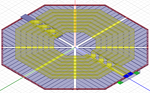
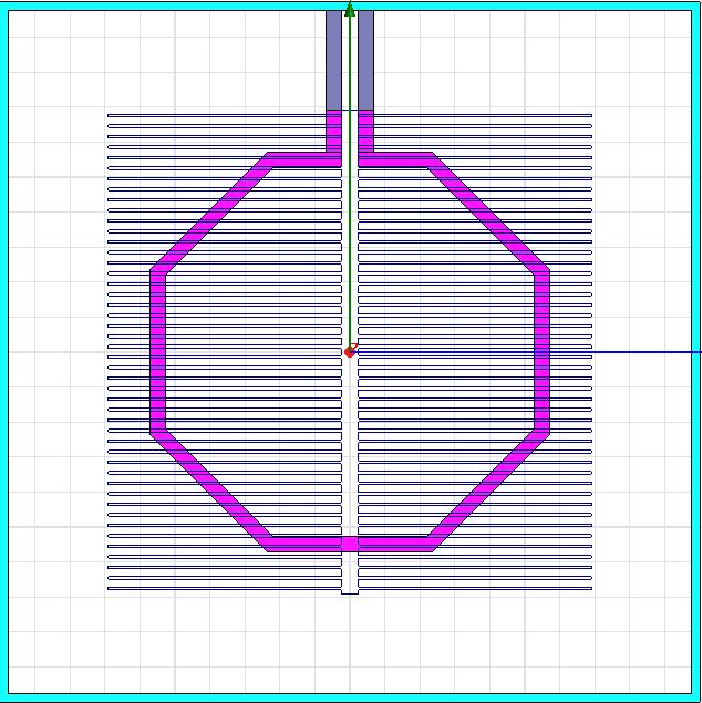
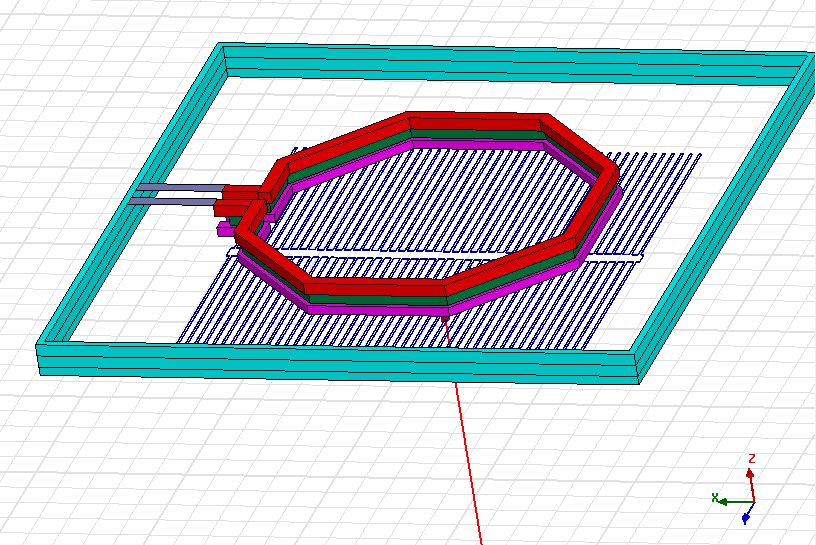
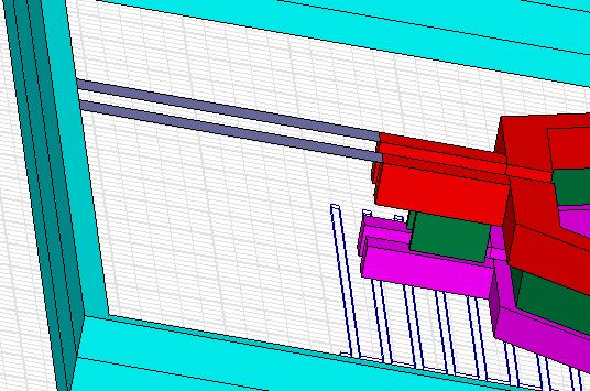
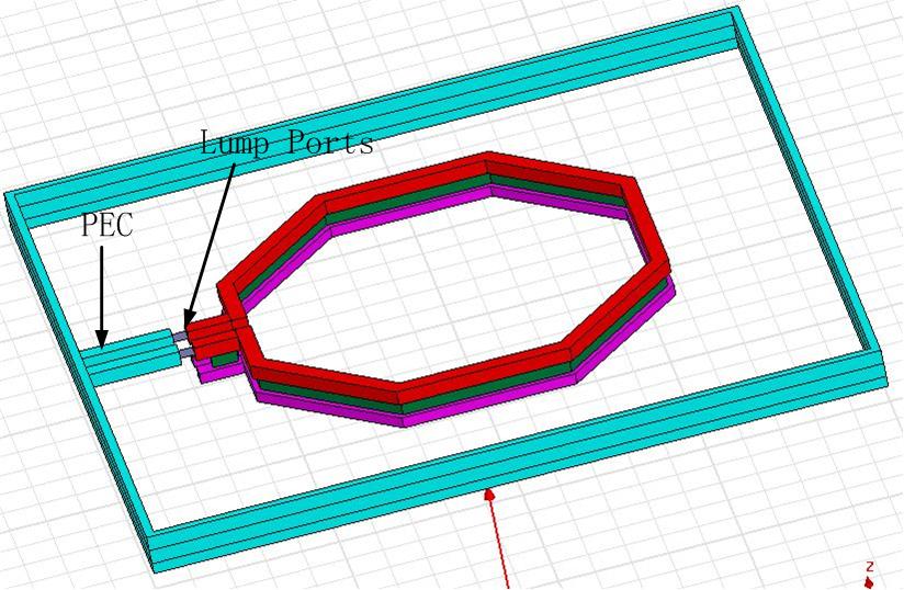
It is a octagonal symmetric inductor in Metal 6 (CMOS technology), with lumped ports: P1 and P2 as two inputs closed to each other. There is also a guard ring on Metal 1, which is also connected to silicon substrate.
If P1&P2 are placed against Metal 1 guard ring directly, the simulation results (S11, or extracted L,Q etc.) looks OK.
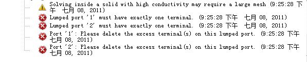
If P1&P2 are against a small piece of PEC, and another port (P3) drives the guard ring against the same PEC, then the S11 changes a lot (e.g. more than half lower self resonating frequency).
Just wondering if anyone have seen this before? Thanks a lot.
 

It's hard to follow the setup ("two inputs closed to each other"?) can you post
the project or at least an image that highlights the ports
 
  • Like
Reactions: bunga

    bunga

    Points: 2
    Helpful Answer Positive Rating
Hi, thanks for reply. I attached the image. The yellow tracks are inductor itself. The red ring is the guard ring in M1, which is connected to the polysilicon shield. The two blue ports (P1&P2) drive the inductor. And the two green rectangles connect the P1&P2 (through a small piece of PEC sheet) and M1 ring.
Now, if the green rectangles are simply PEC sheets, that means the P1&P2 drive the inductor against the M1 ring directly. And the simulation results are fine (i.e. L~15nH, Q~8, SRF~4GHz)
However, if the green rectangles are also lumped ports as P1&P2. Then the S11 shows SRF reduced to ~1.5GHz.
Just wondering how the two ports affect the results?
Thanks very much!
 

Attachments

  • inductor_hfss.png
    inductor_hfss.png
    84.5 KB · Views: 261
  • Like
Reactions: bunga

    bunga

    Points: 2
    Helpful Answer Positive Rating
That's better, but still some questions on gemoetry : This inductor can't be just on
M6; I assume there's another metal layer (M7, AP?...). Also there's gray bar opposite
the ports. Is this a center tapped inductor? Sometimes when you see a factor of two
one suspect is single ended vs differential...
 

Hi, rntsay,
Thanks! The coil is mainly in M6 and there are some small segments in M5 for under lying connections (sorry they are gray...) . Yes, you are right, the other gray track is the centre tap, which could be used as well if I apply another lumped port to it against the M1 guard ring. The main issue is the extra ports for ground connection. Can you see any problems?
 

You can leave the center tap floating if that's what you want. I'm attaching
a good summary that might help you track down the factor of two you're
picking up (pdf freely available on net)
 

Attachments

  • InTech-Modeling_of_spiral_inductors.pdf
    893.7 KB · Views: 343
Hello, I have seen your inductor's model, but I have some questions. First, have you set the thickness of the Metal 6, if you setted up, how to get the lumped prots. Second, does your model exactly with the real one?
Thank you for your reply.
 

Yes, the thickness of M6 is set up already, and just let one edge of lumped ports (a piece of rectangle) attached to vertical face of the inductor input segments. It doesn't matter if you they join at the upper or lower part of the face.
I didn't get your second question.
 

    V

    Points: 2
    Helpful Answer Positive Rating
Yes, the thickness of M6 is set up already, and just let one edge of lumped ports (a piece of rectangle) attached to vertical face of the inductor input segments. It doesn't matter if you they join at the upper or lower part of the face.
I didn't get your second question.

thanks for reply. This is my work, I use MA metal(red one) and the E1 metal(pink one) for the inductor, the vias is the green ones. The cyan one is the guard ring use the MA and E1 metal. Under the inductor, it's a shield using M1. The problem is when I use the lump port (p1&p2), just as the grey ones, which connect the inductor and the guard ring, it always have a mistake. Do you know how to corrected it?
Thank you.


---------- Post added at 15:10 ---------- Previous post was at 15:01 ----------

And in your designs, M6 and M1 should not been in same layer, so how connect the inductor and ground by lump ports.
 
  • Like
Reactions: bunga

    bunga

    Points: 2
    Helpful Answer Positive Rating
The lump ports are too long, it's better to have a low aspect ratio, You could connect one edge of a port to the inductor's arm, the other edge to another long, thin PEC box, which is attached to the internal face of the guard ring.
you can always make connections using PEC objects or boundaries, as long as they are much smaller than, or far enough from the main structures.

what mistakes do you have?


thanks for reply. This is my work, I use MA metal(red one) and the E1 metal(pink one) for the inductor, the vias is the green ones. The cyan one is the guard ring use the MA and E1 metal. Under the inductor, it's a shield using M1. The problem is when I use the lump port (p1&p2), just as the grey ones, which connect the inductor and the guard ring, it always have a mistake. Do you know how to corrected it?
Thank you.


---------- Post added at 15:10 ---------- Previous post was at 15:01 ----------

And in your designs, M6 and M1 should not been in same layer, so how connect the inductor and ground by lump ports.
 
I have tried the PEC's methods, but there are still the same errors, just as the pictures shown. Thank you for your help, may I have your e-mail adress please?


Status
Not open for further replies.

Part and Inventory Search

Welcome to EDABoard.com

Sponsor

Back
Top