Welcome to our site! EDAboard.com is an international Electronics Discussion Forum focused on EDA software, circuits, schematics, books, theory, papers, asic, pld, 8051, DSP, Network, RF, Analog Design, PCB, Service Manuals... and a whole lot more! To participate you need to register. Registration is free. Click here to register now.
If your output transistor is a MOSFET, its parasitic anti-parallel diode will take care of a max. inverse in-out voltage difference of about 1V . In case of a BJT, a small inverse in-out voltage difference (a few volts) won't matter.
If your output transistor is a MOSFET, its parasitic anti-parallel diode will take care of a max. inverse in-out voltage difference of about 1V . In case of a BJT, a small inverse in-out voltage difference (a few volts) won't matter.
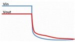
I read somewhere that if input will become less than output, a reverse current may flow in opposite direction which may lead to damage the LDO.
For this particular applicatino a small reverse current may flow for short time and LDO could sustain for that, but still I am not sure.
This site uses cookies to help personalise content, tailor your experience and to keep you logged in if you register.
By continuing to use this site, you are consenting to our use of cookies.