Continue to Site

Welcome to EDAboard.com

Welcome to our site! EDAboard.com is an international Electronics Discussion Forum focused on EDA software, circuits, schematics, books, theory, papers, asic, pld, 8051, DSP, Network, RF, Analog Design, PCB, Service Manuals... and a whole lot more! To participate you need to register. Registration is free. Click here to register now.

Something wrong with Altium

Status
Not open for further replies.

hithesh123

Full Member level 6
Joined
Nov 21, 2009
Messages
324
Helped
1
Reputation
2
Reaction score
1
Trophy points
1,298
Location
lax
Activity points
3,548
Just finished a PCB last week and got it made. To my surprise it had some connection errors.
I checked the schematic and everythings seems to be fine. But the layout has some connection errors.

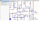
I purposefully disconnected a resistor and compiled the schematic. No Errors!
I disconnected both ends of the resistors. Again no Errors!
(see attachment - R11 is disconnected)

Got a bunch of warnings saying - pin.. has no driving source.

Why is altium not showing the errors.
 

Attachments

  • err.jpg
    err.jpg
    114.4 KB · Views: 68

Altium's PCB Design Rule check will ensure that the PCB matches the schematic's netlist. but to do that:

1) You have to make sure the schematic is correct. the warnings are helpful, but it can't read your mind, and anyway they only flag errors if the pins have their functions defined in the library, and the "connection matrix" (Project -> Project Options -> Connection Matrix) flags the connection as an error. I have seen cases where Altium "helpfully" connected crossing wires on the schematic while I was moving things around, even though I didn't intend that. It put a dot on the connection (which I was able to spot), and I got a warning (luckily the unintended connection violated some rules) but ultimately you need to be sure the schematic is what you want.

2) You need to import any changes from the schematic to the PCB (Design -> Import Changes). Changes don't flow to the PCB until you command it.

3) You need to actually run the Design Rule Check on the PCB (Tools -> Design Rule Check). It might automatically highlight some errors on the PCB, but you need to actually run the DRC and inspect the results to see everything.

If you did those things and your PCB doesn't match the schematic, I can't explain why. My last design had 550 components and the Design Rule Checks did their job perfectly.
 

Kevin54,

1. The schematic is correct. I am aware of the wire-intersection dot and took care since starting the design to avoid unwanted connections.
2. Yes, I imported changes from sch to pcb
3. Ran DRC, got some warnings regarding overlay and pad clearance. No errors.
 

The only thing I can suggest is to generate a netlist from the schematic (Design -> Netlist for Project -> Wirelist, then look under "Netlist Files" under "Generated"). Inspect it manually to see if it matches what you think the schematic says. If it doesn't, the problem is on the schematic side, otherwise it's on the PCB side (which would probably indicate a problem with the design rules).

By the way, disconnecting a resistor doesn't necessarily flag an error (the "Connection Matrix" controls whether or not it does). It could be what you intended, the program can't read your mind. Sometimes I place uncommitted components on PCBs for later tests or modifications. The program is only really at fault if the PCB doesn't match the netlist. So try generating a netlist, which should tell you if the problem is on the schematic or PCB side. If on the schematic side, look for a problem with a footprint or the way you're wiring it up. If on the PCB side, look for a problem with the design rules (which there shouldn't be unless you changed them).
 

Status
Not open for further replies.

Part and Inventory Search

Welcome to EDABoard.com

Sponsor

Back
Top