Continue to Site

Welcome to EDAboard.com

Welcome to our site! EDAboard.com is an international Electronics Discussion Forum focused on EDA software, circuits, schematics, books, theory, papers, asic, pld, 8051, DSP, Network, RF, Analog Design, PCB, Service Manuals... and a whole lot more! To participate you need to register. Registration is free. Click here to register now.

Passing Data From 2*Clk to a domain that is clk

Status
Not open for further replies.

Digital-L0gik

Member level 2
Joined
Jan 26, 2009
Messages
44
Helped
5
Reputation
10
Reaction score
4
Trophy points
1,288
Activity points
1,577
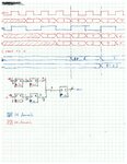
I have data coming at 2*clk and I want to clock the data into half the clock (clk) without losing data. For example, if I have 16 bits coming in at speed 2clk, I want to capture it in domain running at clk and perhaps ouput 32 bits of data in the clk domain, thus capturing two cycles of data coming at 2*clk into the clk domain. Any pointers or examples I can study? Thanks for the help.
 

Maybe the easy way is try to reference the Xilinx FIFO which can be generated coregen with 16bit input (2*clk domain) and 32bit output (clk domain).
 

if two clocks are not phase aligned, search asynchronous and handshake on google, but 2clk cannot pump the data continuously.
If they are phase aligned, it's a simple synchronous design.
 

1 2X flop goes to 2 1X clocks. One 1X clock on rising and one 1X clock on falling. So you king of assume first 2X clock data is captured by pos-edge 1X and 2nd 2X clock data is captured by neg-edge 1X.
 

This is what I came up with, I think it will work but would like some feedback from the community. Thanks for the help. The last two blue signals in the timing diagram are node D and out.
 

Attachments

  • newimage.jpg
    newimage.jpg
    800.8 KB · Views: 119

Did take a look. Was a little confused. Here is the sequence I was thinking about.

stage 0 - 2xclk
stage 1 - 1xclk
stage 2 - 1xclk

stage0 has 1 2x flop launching data bits every clock cycle

stage 1 has 2 1x flops. 1 clocking posedge and 1 clocking negedge.
So if you assume 4ns 1X clock cycle period, both (1x & 2x clocks) rising edges starting at time 0, negedge 1X flop captures first data bit at 2ns, posedge 1x flop captures second data bit at 4ns.

stage 2 - necessary to sync up the 2 data bits.
So here is a tricky part. You have to do a 0-cycle capture from stage 1 posedge flop and half cycle capture from stage 1 negedge flop.
So the stage 2 has 2 1X flops clocked posedge.
Data bit from stage 1 posedge flop is captured by stage 2 posedge flop at 4ns
Data bit from stage 1 negedge flop is captured by stage 2 posedge flop at 4ns.
 

Status
Not open for further replies.

Part and Inventory Search

Welcome to EDABoard.com

Sponsor

Back
Top