Continue to Site

Welcome to EDAboard.com

Welcome to our site! EDAboard.com is an international Electronics Discussion Forum focused on EDA software, circuits, schematics, books, theory, papers, asic, pld, 8051, DSP, Network, RF, Analog Design, PCB, Service Manuals... and a whole lot more! To participate you need to register. Registration is free. Click here to register now.

Need help with Colpitts crystal oscillator

Status
Not open for further replies.

hayowazzup

Advanced Member level 4
Joined
Oct 9, 2010
Messages
117
Helped
0
Reputation
0
Reaction score
0
Trophy points
1,296
Activity points
2,136
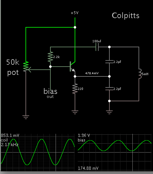
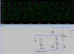
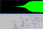
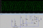
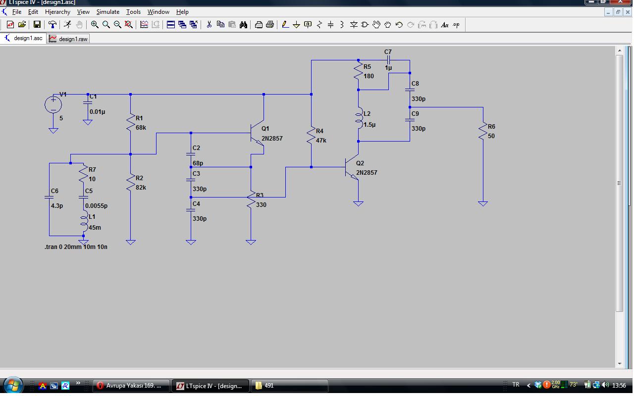
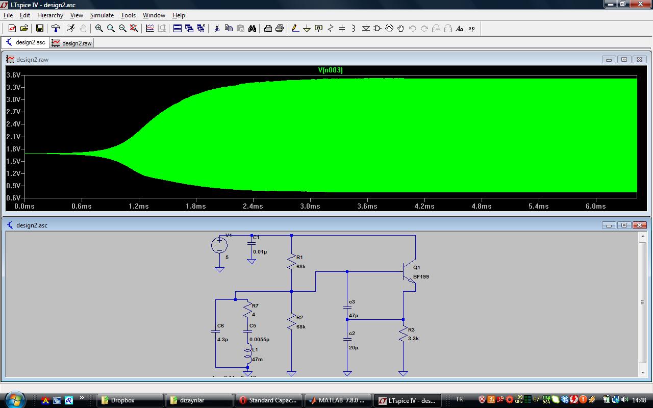
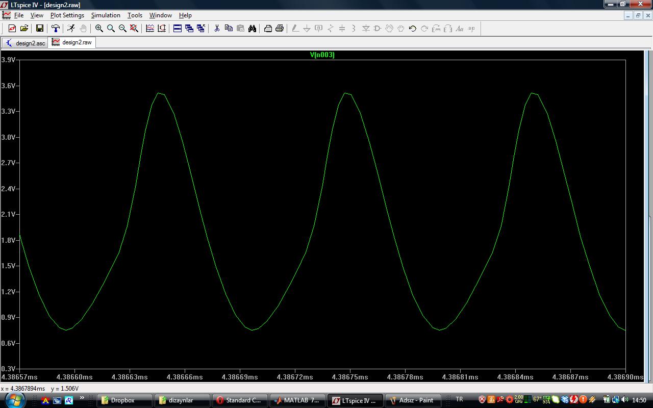
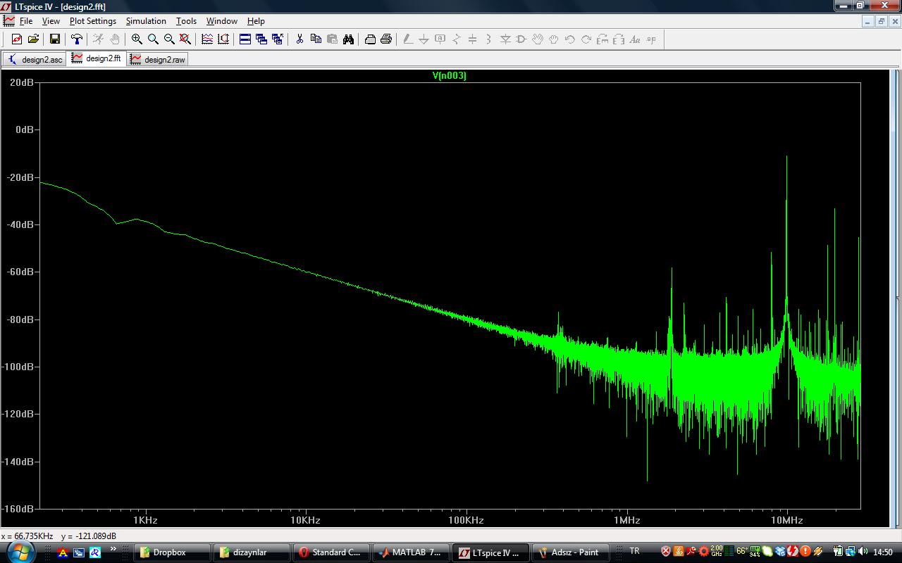
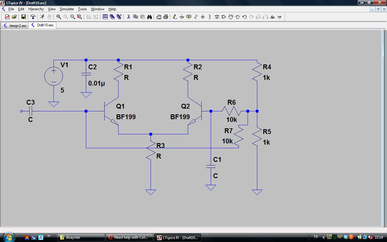
Hi, I would like to know if it is possible to use easy formulas to find out the components' value of this oscillator circuit.
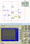
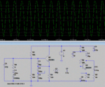
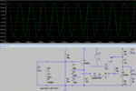
**broken link removed**

ref: **broken link removed**

Are there any general formulaes/easy tricks to analyse this circuit? Or must I going through all the bjt anaylsis and ODE in order to find them out? I already know positive feedback , frequency filtering, etc those sort of stuff.

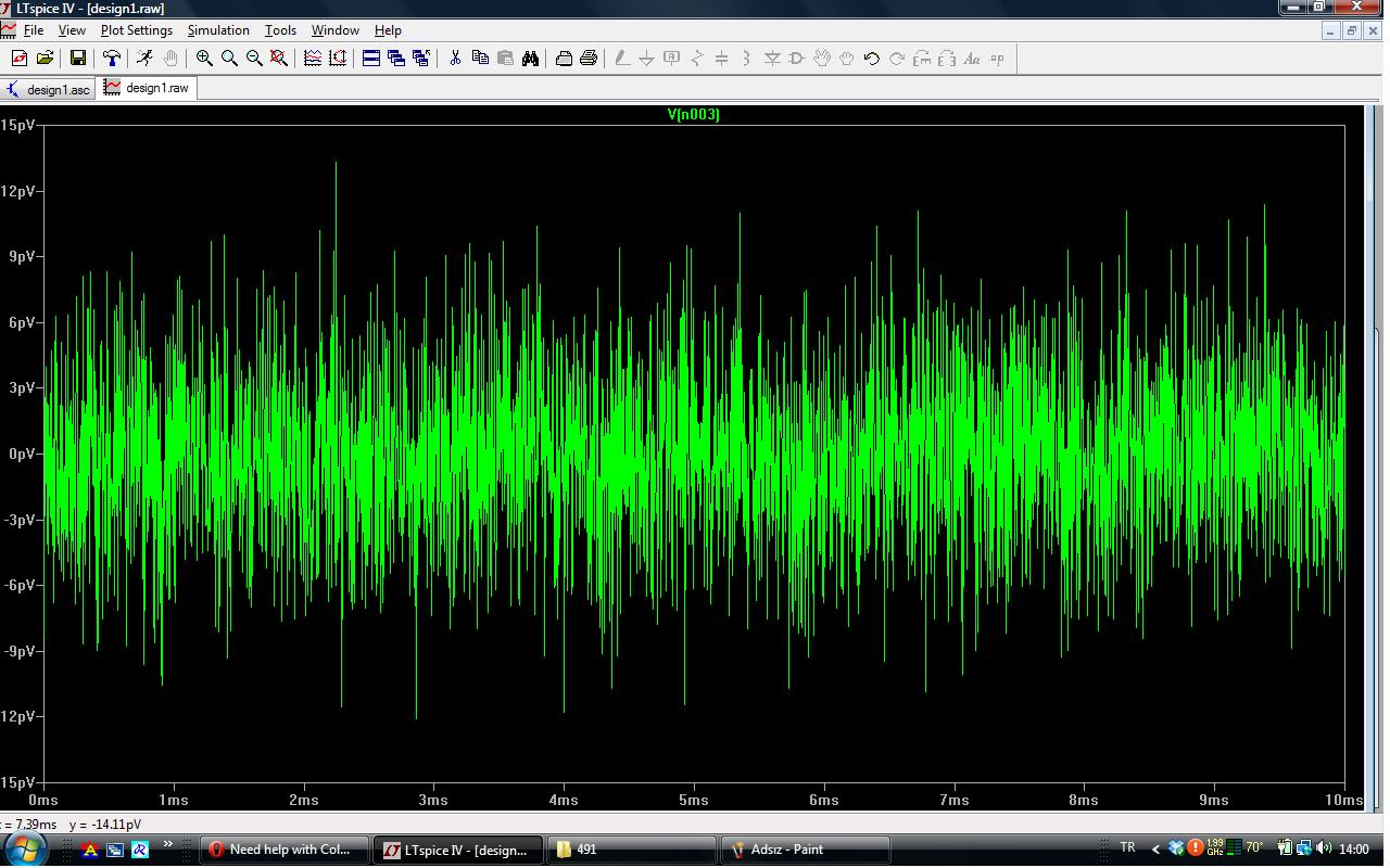
This is actually one of the circuit in my project last semester but all I did was just using Spice to guess them randomly..

What is the easiest way to solve it?i suppose it's the way used by prof engineers.

Your help will be greatly appreciated.. many thanks!
 

I have the same question. Are there any suggestions?
 

Ideally C1 should be a value between (39 – 82)pF. The time constant formed by R3*C2 ~ 0.5/f, where C2 is in uF and f in MHz. Try and keep the value of C2 between (39 - 220)pF for good performance. Practical values for R3 should be between 150 Ohm to about 1k. This will also depend on what the impedance is of the load you are going to connect to the output of the oscillator.
R1,R2 should be calculated to get between 0.2 to 0.5*Vcc on the emitter. The total effect of R1//R2 should be high enough not to load the crystal shunt impedance and degrade Q of the crystal. R2 is often omitted in designs. There is no specific ratio required between the value of C1 and C2.
This is not so much of a problem with a crystal operating at 10MHz or higher. It can become a real problem with, for instance, a watch crystal at 32kHz with a high shunt impedance where even minimal loading will prevent the oscillator from starting up.
At low frequencies, it is better to use a FET instead of a BJT. For a FET based design take R3*C2 ~ 0.3/f.

You may find circuits that are way off these guidelines and still work. These guidelines come from various design literature, my own analysis and design experience for achieving good performing designs.

Be careful of simulating crystal oscillators with circuit simulators. Many simulators don't handle these circuits well due to the high Q of the crystal. It takes long simulation times with small enough time steps to see results. I have seen many crystal oscillator circuits that refuse to simulate but work very well in practice. For serious design work you would look at using a non-linear type simulator.

If we look into the base of the transistor (what the crystal will see) with a network analyzer we see a negative resistance of -15.37 Ohm. Looking at the crystal model we see that this resistance will cancel out the crystal series resistance of 12 Ohm. This is very important. If the circuit does not generate enough negative resistance to overcome the crystal's internal resistance, one of the conditions for oscillation will not be satisfied. To stress this point: A typical 1.5 MHz crystal has an internal resistance of 500 Ohm. So it is clear that these circuit values will not work with such a low value crystal.
 

Attachments

  • crystal_osc_11M.gif
    crystal_osc_11M.gif
    87.1 KB · Views: 211
  • neg_resistance.gif
    neg_resistance.gif
    60.7 KB · Views: 177
Last edited:
  • Like
Reactions: ahmann

    ahmann

    Points: 2
    Helpful Answer Positive Rating
Thank you so much for your help! However i tried the values you gave me and my circuit doesnt start oscillating. Maybe it is because i am using different kind of transistor. Can you check the topic and share your precious ideas for me? thanks
https://www.edaboard.com/threads/268534/
 

In the troubleshooting stage you can expect to do a lot of adjusting. It's all part of the learning process.

Examples:

* The transistor bias may need to be raised or lowered. A potentiometer adjust is just the thing for this.

* A DC blocking capacitor may be needed somewhere.

* You may need to increase or decrease the emitter resistor.

* You may need to add a collector resistor.

* The supply voltage may make a difference.

* To get oscillations started it may need an instigator, kick, touch, shock, etc.

Etc.

This screenshot is an animated simulation of a Colpitts oscillator. It has a coil rather than a crystal. (This simulator doesn't support crystals.)


Notice I had to add a DC blocking capacitor.

I put the LC tank at the right, because that is where the greatest current flow is taking place. One could say the transistor is driving the oscillations. When we re-draw a circuit, it sometimes serves as an aid to comprehension.
 
  • Like
Reactions: ahmann

    ahmann

    Points: 2
    Helpful Answer Positive Rating
Maybe you are not setting up the simulation correct in LT Spice.
I don't have your transistor model in LT, but it works with gen purpose 2N3904.
Waveforms were sampled on the emitter.

Next set shows the results with the buffer added.
 

Attachments

  • 10M_xosc.gif
    10M_xosc.gif
    142.3 KB · Views: 176
  • 10M_xosc1.gif
    10M_xosc1.gif
    156 KB · Views: 165
  • 10M_xosc2.gif
    10M_xosc2.gif
    157.6 KB · Views: 152
  • 10M_xosc3.gif
    10M_xosc3.gif
    180.8 KB · Views: 169
Last edited:
  • Like
Reactions: ahmann

    ahmann

    Points: 2
    Helpful Answer Positive Rating
thank you so much for your interest! I tried the circuit with 2N3904, and it seems working. However, I couldnt get pure sinusoidal and the FFT didnt seem promising.
Then I tried the circuit with 2N2857 which I have to use. In this case the output was not even closer to sinusoidal. I am adding library model for 2N2857 and output wave. I need to get 10 mW on 50 ohm resistor in the end.


******
*SRC=2N2857;2N2857;BJTs NPN; Si; 30V 40.0mA 1000MHz CENTRAL TRANSISTOR
.MODEL 2N2857 NPN (IS=1.55467e-17 BF=296.182 NF=0.850014 VAF=10
+IKF=0.00544635 ISE=2.01913e-14 NE=1.54276 BR=19.550
+NR=0.825166 VAR=73.1109 IKR=0.0544635 ISC=1e-160
+NC=2.9688 RB=21.0221 IRB=0.478136 RBM=0.1384250
+RE=0.000646335 RC=3.0552 XTB=0.582018 XTI=1
+EG=1.06135 CJE=1.08982e-12 VJE=0.99 MJE=0.230
+TF=2.15066e-11 XTF=1000 VTF=1.33967 ITF=0.0010
+CJC=1.89423e-12 VJC=0.95 MJC=0.23 XCJC=0.4084790
+FC=0.1 CJS=0 VJS=0.75 MJS=0.50
+TR=1e-07 PTF=0 KF=0 AF=1)
******
 

In this case the output was not even closer to sinusoidal.
Which is a rather misleading description for a circuit not oscillating at all, isn't it?

Unfortunately, we can't see from the pV waveform if it's a problem of too short simulation time respectively missing "kick-start", or simply a case of too low gain.

I guess, some forum members would be possibly motivated to look into the problem details if you manage to post the (zipped) LTSpice file.
 

Maybe you are not setting up the simulation correct in LT Spice.
I don't have your transistor model in LT, but it works with gen purpose 2N3904.
Waveforms were sampled on the emitter.

Next set shows the results with the buffer added.

Also R4 value should be 4 ohm for Q around 800 K.
 

Also R4 value should be 4 ohm for Q around 800 K.
10 ohm is realistic for industry standard 10 MHz, HC49 case, AT-cut. Miniaturized cyrstals have probably higher Rs.
 

10 ohm is realistic for industry standard 10 MHz, HC49 case, AT-cut. Miniaturized cyrstals have probably higher Rs.
It will be SC cut, 800K min Q, Co=4.3pF,C1=5.5fF, R1=10 ohm max. according to the datasheet. Since freq will be 10 Mhz, I calculated L as 47 mH. To satisfy Q value R must be around 4 ohm
 

O.K., but do you say, the difference matters for the discussed problem?
 

thank you so much for your interest! I tried the circuit with 2N3904, and it seems working. However, I couldnt get pure sinusoidal and the FFT didnt seem promising.

It is not difficult to clean up the waveform if you want. There are several ways to do it. Here are two examples.

The one use a similar 10MHz crystal as a narrow-band filter to clean up the waveform.
 

Attachments

  • 10M_xosc4.gif
    10M_xosc4.gif
    138 KB · Views: 162
  • 10M_xosc_fft.gif
    10M_xosc_fft.gif
    34.8 KB · Views: 146
  • 10M_xosc5.gif
    10M_xosc5.gif
    168.8 KB · Views: 178
Last edited:
  • Like
Reactions: ahmann

    ahmann

    Points: 2
    Helpful Answer Positive Rating
Thanks so much E-desing! I have decided to go step by step to comprehend every details of oscillator design. Firstly, I decided to focus on Colpitts part without buffer. I dont want my transistor to get into SAT state. I designed my circuit by considering what you wrote before. This is the colpitts part.

In the first picture, oscillation didnt seem to be symmetrical with regard to the dc line. Does it mean that transistor is saturated? Or is it the nature of normal oscillation. Do you think that my harmonics are small enough to neglect them?

For the buffer amplifier section, I assume that instead of the buffer design I used before, I will use differential pair. Do you have any suggestions how I can design my circuit?
Thanks in advance!
 

Nonlinearity is required by an oscillator to achieve steady state oscillations. This involves a certain degree of signal distortion respectively harmonics. You can reduce it by carefully adjusting the excess gain to a minimum, varying the capacitor ratio. But the circuit should oscillate reailably with varying temperature and transistor current gain.
 
  • Like
Reactions: LvW

    LvW

    Points: 2
    Helpful Answer Positive Rating
In the first picture, oscillation didnt seem to be symmetrical with regard to the dc line. Does it mean that transistor is saturated? Or is it the nature of normal oscillation.

This goes with the elongation toward the peak of your sinewave. The percentage of voltage gain is greater there, as compared to the trough region where the reduced bias creates less swing. Notice the trough is more rounded.

If you reduce the amount of swing, you will get a more linear sinewave. You will get reduced harmonics. You can maneuver the entire waveform up or down to find the level that yields the best distortion level.

Since you are getting a sinewave, your transistor is not saturating.
 
  • Like
Reactions: ahmann

    ahmann

    Points: 2
    Helpful Answer Positive Rating
Thanks guys. I assume that I am done with Colpitts part. Now Iam working with differential amplifier part. However, It is difficult for me to determine capacitor and resistor values. What values I should use for bypass capacitor connecting my output of colpitts and input of amp for 10 Mhz? Capacitor must be like a short circuit at 10 Mhz. What should I use for c1 and other resistors?
 

Now Iam working with differential amplifier part. However, It is difficult for me to determine capacitor and resistor values. What values I should use for bypass capacitor connecting my output of colpitts and input of amp for 10 Mhz? Capacitor must be like a short circuit at 10 Mhz. What should I use for c1 and other resistors?

The way I have it working in my simulation, this is a phase splitter. Do you wish to obtain two signals, one inverted from the other? (If so then a single transistor can be made to do this.)

Start with 330 ohms for R1-R2.
33 for R3.

Make C1 very small so it does not attenuate your signal. (I was going to suggest that you omit it, but maybe you want it to remove harmonics?)

You need an input resistance, in series with C3. Start at 4700 to 47 k ohms, depending on incoming signal amplitude.

The resistor divider at right should be replaced by a potentiometer. Say, 2k. Both transistors have should their own individual potentiometer so you can custom adjust each bias. It's the only way to center a signal in the region between ground and supply +.
 
Status
Not open for further replies.

Part and Inventory Search

Welcome to EDABoard.com

Sponsor

Back
Top