Continue to Site

Welcome to EDAboard.com

Welcome to our site! EDAboard.com is an international Electronics Discussion Forum focused on EDA software, circuits, schematics, books, theory, papers, asic, pld, 8051, DSP, Network, RF, Analog Design, PCB, Service Manuals... and a whole lot more! To participate you need to register. Registration is free. Click here to register now.

What determinates the CP output voltage for active loop filter

Status
Not open for further replies.

poorren

Junior Member level 3
Joined
Jan 15, 2011
Messages
27
Helped
1
Reputation
2
Reaction score
1
Trophy points
1,283
Activity points
1,654
Hello,
I'm building a frequency synthesiser using a national semi's PLL. Because, the VCO's tuning voltage is out of the range of PLL power supply. I choose to use a type A active filter as attachment.
active_design3a.gif

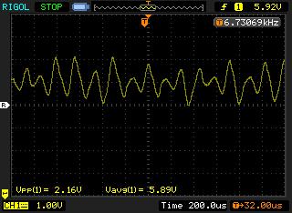
I used National semi's easyPLL to get a loop filter with 3order, and test it in real circuit. I found the voltage of CP (directly connected to OP AMP -) is almost 3.3V, the power supply of PLL, the voltage bias on OP AMP + input has been set to 1.9V. Using Osc Scope, I capture the voltage waveform of CP output, the voltage has short pulse constantly. The pulse has a min voltage 2.8V, max voltage 3.3V. So, I am very confused that what kind of things determinate the voltage of CP? How the current output of CP change to tuning voltage at VCO?

Thanks for your replies and time.
 

As you said, it's a current output, so measuring a voltage without a suitable load doesn't make much sense. What are you exactly searching for?

I would expect open drain N and P current sources. So biasing the integrator somewhere around mid supply, as you apparently did, sounds reasonable. Unlikely, that the datasheet has an exact current versus voltage characteristic for the phase detector output.
 

Thanks for your reply. I found the issue of driving OP AMP - to around 3.3V is the charge pump polarity. The Type A loop filter used here is actually of negative gain. The VCO I used is of positive slope. So, I changed the charge pump current polarity to negative. The loop began to lock. Another issue I found is that the VCO locked frequency output will rock in a small frequency range. The target locked frequency is 190Mhz, the observed frequency will slowly change from 189.7Mhz to 190.2Mhz periodicly. I further measured the tuning voltage of VCO, the below picture is what I captured using OscScope.

10_1295150334.jpg


Obviously, there is ringing in loop filter, my issue now is how to estimate the phase margin and eliminate the ringing there?
 

O.K., I didn't clearly understand from your initial post, that the integrator was saturated - due to wrong loop gain sign.

At first sight, the waveform simply looks like a PLL filter dimensioned inappropriate for your PLL parameters. What's PFD input frequency?
 

O.K., I didn't clearly understand from your initial post, that the integrator was saturated - due to wrong loop gain sign.

At first sight, the waveform simply looks like a PLL filter dimensioned inappropriate for your PLL parameters. What's PFD input frequency?

Thanks for your reply! I made the mistake at initial post on CP polarity. :(
Another progress is made yesterday afternoon on adjustment capacitor near the VCO tuning point. From what I captured, I notice that the ringing on Vtuning is probably due to too low or too high phase margin. My guess is as follows.

The PFD input frequency is 190Mhz, with 1Mhz reference frequency. The datasheet provides the charge pump current at 3.5mA, the tuning sensitivity is at 12Mhz/Voltage. The National Semi's easyPLL syntheses the loop filter with phase margin around 43 degree and the loop filter bandwidth is 3.3Khz. The ringing frequency is about 6 Khz. So, I suspect that the loop gain at 6Khz is not attenuated that enough, below 0dB. Or, the practical parameters have some different than synthesis condition, which leads the phase margin at 0dB bandwidth is not stable value. I tried to change the last stage capacitor and see the total loop PM and BW changes, it proves that the increment on that will decrease the BW and PM. So, I tried to replace a larger capacitor than the initial design(1.5nF -> 4.7nF). The ringing disappears now, I tried to change VCO from 150 Mhz ~ 190Mhz, the tuning voltage is somewhat stable. That proves the PLL is art than science.

I still have issue to consult. How could we estimate the phase margin or BW in circuit. I notice that if we have a method to estimate these values, it will give us great help on tuning the final design.

---------- Post added at 13:40 ---------- Previous post was at 11:44 ----------

O.K., I didn't clearly understand from your initial post, that the integrator was saturated - due to wrong loop gain sign.

At first sight, the waveform simply looks like a PLL filter dimensioned inappropriate for your PLL parameters. What's PFD input frequency?

Another thing I noticed is the spectrum of generated CW have some kind of issue which I couldn't explain.
See below for spectrum I captured.
Screen_0001.png

The target frequency is 200Mhz in this case, I didn't send the reference clock of my board into the spectrum analyzer.
So, there's litter frequency error. But, there are several very high spurs at each side of center frequency which is about 20Khz spaced. In general, the spur is symmetry around the center frequency. I don't know why this happens. My current guess is common noise from analog GND. But I haven't chance to verify this.
What's your idea about my question? Have you met similar issue? Thanks.
 
Last edited:

Operate the VCO open loop to determine if the spurious signal is generated in the PLL loop. If I understand the circuit correctly, disconnecting the phase detector current output should be sufficient to bias the filter to center frequency.

You should also show the full spurious spectrum. It's obviously wider than three lines. The modulation is very clear. If it's caused by an interference, it must be unusually stationary.
 
Last edited:
  • Like
Reactions: MRAMA

    MRAMA

    Points: 2
    Helpful Answer Positive Rating
Operate the VCO open loop to determine if the spurious signal is generated in the PLL loop. If I understand the circuit correctly, disconnecting the phase detector current output should be sufficient to bias the filter to center frequency.

You should also show the full spurious spectrum. It's obviously wider than three lines. The modulation is very clear. If it's caused by an interference, it must be unusually stationary.

Thanks for your feedback! Your idea is good to isolate the issue. I tried yesterday, and got more result, hope to post more in tomorrow.
Yesterday's result is focused on the close-loop performance.
The following picture is what I got from LO driver output, an amplifier after VCO output. The high power of driver output generates many high-order harmonic spur, which extends to very high frequency.

Screen_0012.png

To get into detailed, I took the following picture.

Screen_0016.png

I agree with your idea, it should be the interference or noise, which leads the spur. I found the control interface from digital board, introduce much noise. Then, after the configuration of PLL, I unplug the control interface. The spur doesn't get resolved. I use a OscScope to look at the V tuning point. I could find two kind of noise in V tuning pin, one is high frequency noise, the frequency is the same as VCO output, I'm not sure this is from VCO leakage or it pick up by OscScope's probe. The second is shot time burst noise, which I couldn't find where it comes from. I did try the open loop test in limit case, the spur is improved much better. Because, the use of an active loop filter, I couldn't easily set a stable tuning voltage. Please give me your idea, I will try more this afternoon.
Thanks for your time!
 

Harmonics are no spurious signals, I think. For a digital signal, the first spectrum would be reasonable.

Regarding open loop test, if you didn't change the circuit, this should be true
disconnecting the phase detector current output should be sufficient to bias the filter to center frequency

Generally, I would suggest to use more regular SA settings, that allow the identification of lines without needing a pocket calculator :smile:
Or use the marker feature of your instrument.
 

Harmonics are no spurious signals, I think. For a digital signal, the first spectrum would be reasonable.

Regarding open loop test, if you didn't change the circuit, this should be true


Generally, I would suggest to use more regular SA settings, that allow the identification of lines without needing a pocket calculator :smile:
Or use the marker feature of your instrument.

Refer to the spur, what I meant is really the second picture in previous post.
I made a kludge on the open loop filter, added a resistor divider to OP-AMP output. So, now, I could set a very stable voltage at the tuning pin of VCO.
Then, check the spectrum of fundemental frequency with span of 1Mhz. The spectrum is still of spurious. I was lucky to measure the tuning pin with OscScope.
I found that there's an interference with the same frequency as VCO at tuning pin, the amplitude is of 0.1Vpp, ***!

To clarify the issue, I break every thing on tuning pin, just left a shunt capacitor with charged the voltage. Due to high input impedance of tuning pin, the DC voltage of tuning pin varied very slow. I could use OscScope to check that pin again. The same frequency interference is still there. Now, I guess that interference comes from the VCO leakage to tuning. I'm wondering whether you have found similar issues or whether you agree with on my result.

Note: I also measure the GND near the VCO, the GND is somewhat much clean (in AC) than tuning pin.
 

Status
Not open for further replies.

Similar threads

Part and Inventory Search

Welcome to EDABoard.com

Sponsor

Back
Top