Continue to Site

Welcome to EDAboard.com

Welcome to our site! EDAboard.com is an international Electronics Discussion Forum focused on EDA software, circuits, schematics, books, theory, papers, asic, pld, 8051, DSP, Network, RF, Analog Design, PCB, Service Manuals... and a whole lot more! To participate you need to register. Registration is free. Click here to register now.

How to calculate BJT NPN transistor using beta?

Status
Not open for further replies.

Rumieus

Junior Member level 2
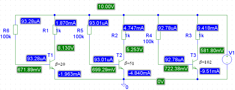
Joined
Jul 7, 2008
Messages
22
Helped
0
Reputation
0
Reaction score
0
Trophy points
1,281
Activity points
1,442
Ib=V1/R1 = 0.1mA
Ic=V1/R2 = 10mA
β=100

Am i right?

In designing circuit, do we calculate Ic using β or using the V=IR because in book which im currently studying, all the calculation are using β to calculate Ic but if β is 50 and then the Ic is different right?

Im just so confuse with electronic..

What are the different between dis 2 circuit?
 

bjt npn transistors

Well
Ib=(V1-Vbe)/R1=(10V-0.65V)/100KΩ≈93.5uA
If BJT work in active region Ic is equal
Ic=Ib*β=93.5uA*β
So if our BJT has β=60 Ic will by
Ic=93.5uA*60=5.61mA. But if our bjt has β=100 then Ic=9.35mA and transistor will be working in saturation region. Because Icmax=V1/R2=10mA
 

npn transistor sizez

In circuit 1, there is no β so how you calculate Ic? V=IcR right?
 

bjt npn transistor

You look in the datasheet 2N4014
**broken link removed**
And then Hfe=β≈70 (Ic around 10mA)
 

bjt transistor β=100 multisim

if β = 70, the the Ic = 7mA.

But how about this? Can some one explain.[/b]
 

npn transistor calculation

Hmm, You know in a real word Ic will still have different value then it is in the simulation. Because we don't know the β of a 2N4014 we can only assume that β is smaller or equal 70.
In you're simulation the BJT is in saturation region because the β is larger the 100 and in the saturation the Ic=Ib*β don't hold anymore
In saturation Ic=(Vcc-vce(sat))/Rc
And that's why we use this circuit only as a switch.
If we want a linear amplifier we use this circuit
https://upload.wikimedia.org/wikipedia/commons/2/27/Common_Emitter_amplifier.png
Ic=[β*(Et-Vbe)]/(Rb+(β+1)*R4)
Et=[R2/(R1+R2)]*Vcc
Rb=R1||R2
|| - parallel Rb=(R1*R2)/(R1+R2)
And assume that Ic=1mA; Vcc=10V;β=70 and VR4=1V
VR3=(Vcc-VR4)/2=4.5V.
R3=4.5V/1mA=4.5K=4.7KΩ
R4=1V/1mA=1KΩ
R2=(VR4+Vbe)/(Iz)=5.1KΩ
Iz=5...30*(Ic/β)
R1=(Vcc-Vbe-VR4)/(Iz+Ib)=24KΩ
check this values in the simulation
 

vbe ic npn transistors

It is a horrible circuit that depends on the unknown actual value of the current gain or of the saturation voltage loss of the transistor.

Real transistor circuits have a voltage divider or negative feedback from the collector to the base for biasing. An emitter resistor is also used.
 

bjt npn data

Real transistor circuits have a voltage divider or negative feedback from the collector to the base for biasing. An emitter resistor is also used
.

Yes, in most cases. The purpose of the circuit hasn't been mentioned at all. So we don't even know, if saturation is intended (for a switch) or shall be avoided (for a linear amplifier). In the latter case, you probably try to achieve a particular operating point, but you didn't tell.

It didn't come clear, why Multisim uses the maximum current gain for 2N4014 rather than a typical value. But it's O.K. in so far, as a current gain of this size has to be considered. To check the circuit stability against parameter variations, the complete min to max range should be tested. Then the measures mentioned by Audioguru get important.

β, by the way, is usually the symbol for the small signal current gain and not identical to large signal value B, that is determining the operation point, altough the difference may be neglected in a rough estimation.
 

saturation region of bjt + wikipedia

Rumieus said:
Ib=V1/R1 = 0.1mA
Ic=V1/R2 = 10mA
β=100
Im just so confuse with electronic..

Hello rumieus,

I am pretty sure you are confused now about all the formulat stuff.
Therefore, my recommendation:
At first, you should always have in your mind that transistor circuits are non-linear circuits - with the consequence that you carefully have to discriminate between static and dynamic (differential) resistances. Your circuit is a mixture of both - resistor as separate parts are static, but transistor pathes (for exampe between base and emitter) exhibit dynamic resistances. Therefore, you need characteristic curves from the data sheet for computing currents and voltages - or you can make suitable assumptions because some parameters are typical for all transistors.
As an example - to assume app. 0.7 volts between base and emitter for normal transistor operation as an amplifier.
And realize - perhaps with the help of a simplified transistor equivalent circuit diagram - that the transistor acts like a voltage controlled current source .
Without these basic considerations you cannot understand and analyze transistor circuits.
 

Status
Not open for further replies.

Part and Inventory Search

Welcome to EDABoard.com

Sponsor

Back
Top