Continue to Site

Welcome to EDAboard.com

Welcome to our site! EDAboard.com is an international Electronics Discussion Forum focused on EDA software, circuits, schematics, books, theory, papers, asic, pld, 8051, DSP, Network, RF, Analog Design, PCB, Service Manuals... and a whole lot more! To participate you need to register. Registration is free. Click here to register now.

How to read\write data using asynchronous clk?

Status
Not open for further replies.

xtcx

Advanced Member level 1
Joined
Dec 22, 2007
Messages
493
Helped
65
Reputation
130
Reaction score
58
Trophy points
1,308
Location
Bangalore, India
Activity points
5,003
hi friends!, I have an issue where my codec sends and receives data at 2MHZ sclk(codec internal) clk.It acts as master and hence the sclk@2MHz isn't controllable by external means. I'll explain in steps.
1) I read\write codec @2MHz sclk(codec clk,master) at the same time on sdi&sdo
2) codec writes 32-bit data to Tx_buffer and reads 32-bits data to Rx_buffer(in FPGA)
3) After reading 32-bits(1 frame) in 16us,the codec goes to idle till 64us.
4) This idle time is to match the sampling time which is 16KHz(64us).
5) The codec reads\writes data @2MHz only or it won't work
6) READ: At 17us,after codec stops writing\reading,I start reading from Tx_buffer (parallel to serial) @1Mbps using FPGA clk @1MHz. So finally I complete my operation at 48us.Remaining 16us is free
7) WRITE: At 17us,after codec stops writing\reading,I start writing to RX_buffer (serial to parallel)@1Mbps using FPGA clk@1MHZ. Again I finish it within 48us.
8 ) BOTH 1MHz read\write to Tx_buffer and Rx_buffer happens from 17us to 48us(32-bits @ 1MHz).
9) This routine is forever.
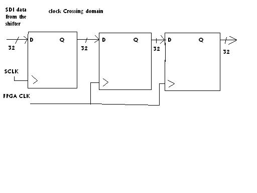
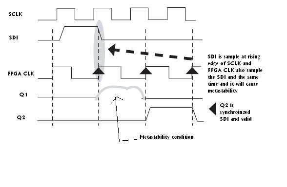
The issue here is that since the codec's clock 2MHz is not accurate when compared to FPGA clk,the FPGA clock shifts faster than codec clk. As a result I find my data missing somewhere...If I simply replace the FPGA 1MHz by codec's (2MHz\2 = 1MHz) 1MHz clk,then I'm able to get my correct audio output...What couldbe the exact reason?....Is this the problem of asynchronous operation?....Isn't the clocks synczing properly?....If every operation is being done using codec Sclk,then I find no problems.
Does anybody have faced this issue? or have any idea related to this?...Does using FIFO could solve this?.....Thanks
 

most likely it was due to the clock synchronization issue between the sclk and the FPGA clock.

could you post part of your code here so that we can analyze abut the data crossing diff clock domain.
or u can email me at ycherjier@yahoo.com so that i can look in details and discuess here.

there is a simple way where using 2 FF to do the data sync with 2 diff clock.
 

Here is my complete code...You can safely omit the statements corresponding to STATE = s0.Si9nce these are only codec initialization steps
Only statements from STATE <= S1 sequence are needed...My explanations at the end of this code...


library IEEE;
use IEEE.STD_LOGIC_1164.ALL;
use IEEE.STD_LOGIC_ARITH.ALL;
use IEEE.STD_LOGIC_UNSIGNED.ALL;


-------------------- ENTITY DECLARATION -------------------------
entity SDR_PSK is
PORT (
clk : IN STD_LOGIC;
sclk : in std_logic;
sw2 : IN STD_LOGIC;
sdofs : in std_logic;
sdo : in std_logic;
rst : out std_logic;
se : inout std_logic;
sdi : out std_logic;
sdifs : out std_logic;
---------
LED : OUT STD_LOGIC_VECTOR(15 DOWNTO 0):=x"0000";
-- clk_sdata_op : OUT STD_LOGIC;
-- clk_data_op : OUT STD_LOGIC;
-- ----------
Txb : OUT STD_LOGIC;
-- Rxb : OUT STD_LOGIC;
INT_OP : OUT STD_LOGIC;
TEST_OP : OUT STD_LOGIC
-- sdofs_op : OUT STD_LOGIC
);
end SDR_PSK;
------------------------ SIGNALS DECLARATION --------------------------------------
architecture Behavioral of SDR_PSK is
-----------CODEC-------------
TYPE main is (s0, s1);
SIGNAL state : main;

TYPE INTERRUPTS1 IS (NONE,SYNC_ON,SYNC_OFF);
SIGNAL INTERRUPT : INTERRUPTS1:= NONE;
--SIGNAL INTERRUPT : INTEGER :=0;
SIGNAL sig : INTEGER RANGE 0 TO 188 :=1;
SIGNAL sig1,t : INTEGER RANGE 0 TO 150 :=0; -- Must start with 0
signal Rx_buff1,Rx_buff2 : std_logic_vector(15 downto 0):="0000000000000000";
signal Tx_buff1,Tx_buff2 : STD_LOGIC_VECTOR(15 downto 0):="0000000000000000";
signal Tx1,Tx2,Tx : STD_LOGIC_VECTOR(31 DOWNTO 0);
signal Rx1,Rx2,Rx : STD_LOGIC_VECTOR(31 DOWNTO 0):=x"00000000";
signal enab : std_logic:='0';
constant ca1 : std_logic_vector(15 downto 0) := x"8901";
constant ca2 : std_logic_vector(15 downto 0) := x"8101";
constant ca3 : std_logic_vector(15 downto 0) := x"8a7b";
--------MARKER----------
----SIGNAL MARKER1 : STD_LOGIC_VECTOR(31 DOWNTO 0):="01111110011111100111111001111110";
SIGNAL MARKER1 : STD_LOGIC_VECTOR(15 DOWNTO 0):="0111111001111110";
SIGNAL DATA_Tx,DATA_Rx : STD_LOGIC;
SIGNAL TEST_REG : STD_LOGIC_VECTOR(31 DOWNTO 0):=x"AAAAAAAA";
----SIGNAL BUFFER_Tx : STD_LOGIC_VECTOR(47 DOWNTO 0);
SIGNAL BUFFER_MARKER,dummy : STD_LOGIC_VECTOR(15 DOWNTO 0);
SIGNAL FLAG_RAMSWAP : STD_LOGIC:='0';
SIGNAL BUFFER_Tx,BUFFER_Rx : STD_LOGIC_VECTOR(31 DOWNTO 0);
--
--------------CODING-----------
SIGNAL CLK_RECOV_PRE : STD_LOGIC;
SIGNAL Mnchr_Rx,Mnchr_Tx,MONOSHOT_inv : STD_LOGIC;
SIGNAL Mnchr_Rx_inv,Mnchr_Rx_delay : STD_LOGIC;
SIGNAl CLK_RECOV,CLK_RECOV_inv : STD_LOGIC;
SIGNAL A,B,C,D,E,F,G,H,X : STD_LOGIC;
SIGNAL A1,B1,C1,D1,E1,F1 : STD_LOGIC;
SIGNAL MONOSHOT : STD_LOGIC;
SIGNAL m,n,o,m1,n1 : INTEGER:=0;
SIGNAl clk_data,clk_sdata : STD_LOGIC;


--
----------------------- PREDEFINED ASSIGNEMENTS ----------------------------------------------------
BEGIN
-----CODING AND MARKER---
--Txb <= DATA_Tx;
--Rxb <= DATA_Rx;
--clk_sdata_op <= clk_sdata;
--clk_data_op <= clk_data;
DATA_Rx <= DATA_Tx;
------------------------------------------------------------------------------------------------------------------------
-- 1. C O D E C I N T E R F A C E M O D U L E
-----------------------------------------------------------------------------------------------------------------------
process(clk,sclk,state,sw2,sdofs,se,enab)
VARIABLE i,i1 : INTEGER:=0;
VARIABLE j : iNTEGER := 0;
VARIABLE temp,temp2 : STD_LOGIC:='0';

begin
----------------------------------------------------------------------------------------------------------------
IF(sw2 = '0') THEN
sig <= 0;
state <= s0;
sig1 <= 0;
IF(enab = '0') THEN
se <= '0';
rst <= '0';
enab <= '1';
ELSIF(enab = '1') THEN
se <= '1';
rst <= '1';
enab <= '1';
end if;
ELSIF rising_edge(sclk) then
enab <= '0'; -- Allow the loop to pass next time
-----------------------------------------------
-- CONTROL WORD CONFIGURATION
-----------------------------------------------
-----------------------------------------------
-- Control Word 1
-----------------------------------------------
case state is
when s0 =>
sig <= sig + 1;
case sig is

when 1 => sdifs <= '1';
when 2 => sdifs <= '0';
sdi <= ca1(15);
when 3 => sdi <= ca1(14);
when 4 => sdi <= ca1(13);
when 5 => sdi <= ca1(12);
when 6 => sdi <= ca1(11);
when 7 => sdi <= ca1(10);
when 8 => sdi <= ca1(9);
when 9 => sdi <= ca1(8);
when 10 => sdi <= ca1(7);
when 11 => sdi <= ca1(6);
when 12 => sdi <= ca1(5);
when 13 => sdi <= ca1(4);
when 14 => sdi <= ca1(3);
when 15 => sdi <= ca1(2);
when 16 => sdi <= ca1(1);
when 17 => sdi <= ca1(0);

--------------------------------------------
-- Control Word 2
--------------------------------------------
when 18 => sdifs <= '1';
when 19 => sdifs <= '0';
sdi <= ca2(15);
when 20 => sdi <= ca2(14);
when 21 => sdi <= ca2(13);
when 22 => sdi <= ca2(12);
when 23 => sdi <= ca2(11);
when 24 => sdi <= ca2(10);
when 25 => sdi <= ca2(9);
when 26 => sdi <= ca2(8);
when 27 => sdi <= ca2(7);
when 28 => sdi <= ca2(6);
when 29 => sdi <= ca2(5);
when 30 => sdi <= ca2(4);
when 31 => sdi <= ca2(3);
when 32 => sdi <= ca2(2);
when 33 => sdi <= ca2(1);
when 34 => sdi <= ca2(0);

----------------------------------------------
-- Control Word 3
-----------------------------------------------
when 35 => sdifs <= '1'; -- CONTROL REGISTER C
when 36 => sdifs <= '0';
sdi <= ca3(15);
when 37 => sdi <= ca3(14);
when 38 => sdi <= ca3(13);
when 39 => sdi <= ca3(12);
when 40 => sdi <= ca3(11);
when 41 => sdi <= ca3(10);
when 42 => sdi <= ca3(9);
when 43 => sdi <= ca3(8);
when 44 => sdi <= ca3(7);
when 45 => sdi <= ca3(6);
when 46 => sdi <= ca3(5);
when 47 => sdi <= ca3(4);
when 48 => sdi <= ca3(3);
when 49 => sdi <= ca3(2);
when 50 => sdi <= ca3(1);
when 51 => sdi <= ca3(0);
state <= s1;
sig1 <= 0;
when others =>
end case;
-------CODEC INITIALIZATION PROCESS COMPLETES --------------------------------------------
-------------------------------------------------
-- DATA BUFFER IN & OUT ( This is a forever loop)
-------------------------------------------------
WHEN s1 =>
sdifs <= sdofs;
sig1 <= sig1 + 1;
case sig1 is
WHEN 0 =>

IF(sdofs = '1') THEN
sig1 <= 1;
ELSIF(sdofs = '0') THEN
sig1 <= 0;
END IF;

WHEN 1 => sdi <= Tx_buff1(15);
Rx_buff1(15) <= sdo;
INTERRUPT <= SYNC_ON;
WHEN 2 => sdi <= Tx_buff1(14);
Rx_buff1(14) <= sdo;
WHEN 3 => sdi <= Tx_buff1(13);
Rx_buff1(13) <= sdo;
WHEN 4 => sdi <= Tx_buff1(12);
Rx_buff1(12) <= sdo;
WHEN 5 => sdi <= Tx_buff1(11);
Rx_buff1(11) <= sdo;
WHEN 6 => sdi <= Tx_buff1(10);
Rx_buff1(10) <= sdo;
WHEN 7 => sdi <= Tx_buff1(9);
Rx_buff1(9) <= sdo;
WHEN 8 => sdi <= Tx_buff1(8);
Rx_buff1(8) <= sdo;
WHEN 9 => sdi <= Tx_buff1(7);
Rx_buff1(7) <= sdo;
WHEN 10 => sdi <= Tx_buff1(6);
Rx_buff1(6) <= sdo;
WHEN 11 => sdi <= Tx_buff1(5);
Rx_buff1(5) <= sdo;
WHEN 12 => sdi <= Tx_buff1(4);
Rx_buff1(4) <= sdo;
WHEN 13 => sdi <= Tx_buff1(3);
Rx_buff1(3) <= sdo;
WHEN 14 => sdi <= Tx_buff1(2);
Rx_buff1(2) <= sdo;
WHEN 15 => sdi <= Tx_buff1(1);
Rx_buff1(1) <= sdo;
WHEN 16 => sdi <= Tx_buff1(0);
Rx_buff1(0) <= sdo;

WHEN 17 => sdi <= Tx_buff2(15);
Rx_buff2(15) <= sdo;
WHEN 18 => sdi <= Tx_buff2(14);
Rx_buff2(14) <= sdo;
WHEN 19 => sdi <= Tx_buff2(13);
Rx_buff2(13) <= sdo;
WHEN 20 => sdi <= Tx_buff2(12);
Rx_buff2(12) <= sdo;
WHEN 21 => sdi <= Tx_buff2(11);
Rx_buff2(11) <= sdo;
WHEN 22 => sdi <= Tx_buff2(10);
Rx_buff2(10) <= sdo;
WHEN 23 => sdi <= Tx_buff2(9);
Rx_buff2(9) <= sdo;
WHEN 24 => sdi <= Tx_buff2(8);
Rx_buff2(8) <= sdo;
WHEN 25 => sdi <= Tx_buff2(7);
Rx_buff2(7) <= sdo;
WHEN 26 => sdi <= Tx_buff2(6);
Rx_buff2(6) <= sdo;
WHEN 27 => sdi <= Tx_buff2(5);
Rx_buff2(5) <= sdo;
WHEN 28 => sdi <= Tx_buff2(4);
Rx_buff2(4) <= sdo;
WHEN 29 => sdi <= Tx_buff2(3);
Rx_buff2(3) <= sdo;
WHEN 30 => sdi <= Tx_buff2(2);
Rx_buff2(2) <= sdo;
WHEN 31 => sdi <= Tx_buff2(1);
Rx_buff2(1) <= sdo;
WHEN 32 => sdi <= Tx_buff2(0);
Rx_buff2(0) <= sdo;

WHEN 33 =>
Tx_buff1 <= Rx(31 DOWNTO 16);
Tx_buff2 <= Rx(15 DOWNTO 0);
Tx(31 DOWNTO 16) <= Rx_buff1;
Tx(15 DOWNTO 0) <= Rx_buff2;
led <= Tx_buff1;
WHEN 100 => INTERRUPT <= SYNC_OFF;
WHEN 126 => sig1 <= 0;
WHEN OTHERS => NULL;
END CASE;
when others =>
end case;
end if;
END PROCESS;

-----------------------------------------------------------------------------------------------------------------------------
-------- 2. M A R K E R A N D B I T S T U F F I N G
-----------------------------------------------------------------------------------------------------------------------------
PROCESS(clk_sdata,clk_data,clk,sclk) IS
VARIABLE i,i1 : INTEGER:=0;
VARIABLE temp,temp2 : STD_LOGIC:='0';
VARIABLE FLAG_LOOP : STD_LOGIC:='1';
BEGIN
---------------------------------
---- CODEC CLOCK GENERATOR @1MHz
---------------------------------

IF RISING_EDGE(clk) THEN
i1:= i1+1;
IF (i1 = 40) THEN
temp2 := NOT(temp2);
clk_data <= temp2;
i1:= 0;
END IF;
END IF;
---------------------------------
CASE INTERRUPT IS
WHEN SYNC_ON =>
C: IF RISING_EDGE(clk_data) THEN

-- IF(INTERRUPT = SYNC_ON) THEN
INT_OP <= '1';
m1<=m1+1;
n1<=n1+1;
IF(m1>=0 AND m1<=30) THEN
Data_Tx <= Tx(m1); --convertuing Buffer data to serial
Rx <= Data_Rx(m1);
ELSIF(m1=31) THEN
Data_Tx <= Tx(m1); --convertuing Buffer data to serial
Rx <= Data_Rx(m1);
END IF;
-- ELSIF(INTERRUPT = SYNC_OFF) THEN
WHEN SYNC_OFF =>
m1 <= 0;
INT_OP <= '0';
WHEN OTHERS => NULL;
END CASE;
END IF;
-- END IF;
END PROCESS;
End Behavioral;
---------------------------------------------------------------------------------------------------------
While the COdec loop of STATE = S1 is a forever loop, which collects data from SDO (as well as writes data to SDI)and stores it temporarily in Rx_buff1&Rx_buffer2(Lch&Rxh),Tx_buff1&Tx_buff2 resp.Totally 32 bits. At the count of 33(sig1) I will pass this temp buffer Rx_buff1&2 to Tx and Tx_buff1&2 to Rx. So Rx and Tx are 32-bit buffer each which holds codec data.(Tx is read data from codec whereas Rx is the data to be written to codec).Any operations that have been done so far are only done under CODEC's SCLK. ALL CODEC read\write operations have been coded under "rising_edge(sclk)",where the SCLK is generated by the codec itself asynchronouly at 2MHz. So all operations execute at 2MHz. Now I need to read\write data from Tx and Rx resp using a 1MHz clk to get 1mbps data rate.That is I need to convert 2mbps data to a constant 1mbps rate....For 1MHz I generated it from my 80MHz FPGA master clk input which is under "Marker and Bit stuffing".Now here comes the problem...The data which we read from FPGA's 1MHz clk is not in phase or exactly the same with sclk. I checked it by dividing 1MHz from SCLK(codec clk) and cross-checked and compared with my FPGA generated 1MHz clk. Both are not same at all..It appears like the codec clk is not 1MHz but some 999.1MHz..As a result,I can see my FPGA 1MHz clk shifting faster than Sclk@1MHz in CRO clearly...Here the term "interrupt" is to generate a flag exaclty at the time when codec read\write starts...So I place my data at the same time inorder to avoid data-missing..The overseen view here is that I must quickly place my data within Interrupt = SYNC_ON.....Well if you have any doubts related,just ask....Thanks for your interests!.....
 

You should use dual clock fifo!
 
  • Like
Reactions: balaceb

    xtcx

    Points: 2
    Helpful Answer Positive Rating

    balaceb

    Points: 2
    Helpful Answer Positive Rating
Hi, sorry..i'm not familiar to VHDL but i think i can roughly guess what the code do.

i have draw a block diagram that discrib your system. hope i didn't get it wrong.

will, i have a doubt, you mention this "After reading 32-bits(1 frame) in 16us,the codec goes to idle till 64us."

that mean initially, the first 32 sclk clock will transfering valid data from codec to FPGA then after the first 32 clock the codec will go in idle state for 64us there the
FPGA will collect the data after the first 32 sclk clock and shift it out at 1MHz.

so my question is what is the condition when the codec get in to idle? did you see sclk still trasmiting?
my guess is it should not trasmiting any signal and always stay high or low for around 64us.

on the other side, what about the 1MHz side, you wan the signal continously trasmiting or it can be stop for some period and retransmit once data is ready?

from my point of view, the sclk from codec will halt for 64us which is long enough for you to transmit the data out at 1mhz.

i have attach a document and you may look for figure 3 and figure 4.


hope it helps....
 

    xtcx

    Points: 2
    Helpful Answer Positive Rating
Sorry for my late response...First I thank you for your interests!
cherjier said:
so my question is what is the condition when the codec get in to idle? did you see sclk still trasmiting?....
For everythin,you have got it correct friend,the codec only accepts or sends data only from 1 to 16us time of 64us frame time. Remaining 48us is the idle time at which I should read the data from the buffer @1mbps.The codec SCLK is always available....Only frame sync appears at 1us(ch1) and another at 8us(ch2).Right after the 2nd frame sync,the data will be taken as 2nd channel data...2 frame sync appears for frame at 1us and 8us.....Well, my issue here is that the codec is master which in the sense,the data and clk timming is not controllable in FPGA...How could you read a data from a different clk domain unless you sync?...No fifo here,coz the data reading\writing action takes place simultaneously...

Added after 1 minutes:

And thanks for your links....Though its useful for my design or not,but helpful for many designs require communication between asyn clk.
 

Well, my issue here is that the codec is master which in the sense,the data and clk timming is not controllable in FPGA...How could you read a data from a different clk domain unless you sync?...

you have to implement a sync circuit to sync the data from the sclk domain to fpga clock domain to avoid metastability issue.

i have draw a simple block diagram for the CDC circuit:


besides, you can implement a counter to count the number of bit the SDI have been receive, this counter can used to generate control signal or handshaking signal and it is usefull for crossing different clock domain.

i have writen a simple code it give you a rought idea how data can be use on the different clock domain, but sorry the code is in verilog, sorry, i not familiar in VHDL.:cry:

Code:
module sclk_sync (
	SCLK,
	SDI,
	SDO,
	
	CLK,
	DATAIN,
	DATAOUT,
	
	RESET_N
	);
	
input			SCLK;			//Codec clock
input			SDI;
output			SDO;
	
input			CLK;			//FPGA CLOCK
input			DATAIN;
output			DATAOUT;
	
input			RESET_N;

//******** Register *******************//
reg		[31:0]	sdi_reg;
reg		[6:0]	counter;		// count to 127 (500ns x 128 = 64us) counter for the entire frame of sclk

reg				sda_rdy;		// to be safe, this signal is the sda data ready condition signal and will be pass over the CDC circuit
reg		[31:0]	dataout_reg;

wire			sda_rdy_sync;
wire			sda_rdy_sync_d1;
wire	[31:0]	sdi_reg_sync;

//data ready start pulse in fpga clock domain (might need to delay for few CLK cycle,depand on design)
wire	data_rdy = sda_rdy_sync & !sda_rdy_sync_d1;  

assign	DATAOUT = dataout_reg[31];		//assume only,should put in start,and stop condition 

// shift register for SDI
always @(posedge SCLK or negedge RESET_N)
	if (!RESET_N)
		sdi_reg <= 32'h00000000;
	else if (!counter[5] && !counter[6])
		sdi_reg <= {sdi_reg[30:0],SDI};

always @(posedge SCLK or negedge RESET_N)
	if (!RESET_N)
		counter <= 7'b0000000;	
	else
		counter <= counter + 1;	
		
always @(posedge SCLK or negedge RESET_N)
	if (!RESET_N)
		sda_rdy <= 1'b0;
	else if (counter == 7'b0000000)
		sda_rdy <= 1'b0
	else if (counter[5] || counter[6])
		sda_rdy <= 1'b1;
		
//sync the sda_rdy signal with the fpga clock,CLK		
sync	sync_u0(
	.CLK	(CLK),
	.RSTN	(RESET_N),
	.D		(sda_rdy),	
	.Q1		(),
	.Q2		(sda_rdy_sync)
	);		
		
always @(posedge CLK or negedge RESET_N)
	if (!RESET_N)
		sda_rdy_sync_d1 <= 1'b0;
	else
		sda_rdy_sync_d1 <= sda_rdy_sync;	
		
//sync the sdi data register to FPGA clock domain
sync	#(32) sync_u1(
	.CLK	(CLK),
	.RSTN	(RESET_N),
	.D		(sdi_reg),	
	.Q1		(),
	.Q2		(sdi_reg_sync)
	);				
		 
// register the sdi_reg_sync for the dataout shifter
always @(posedge CLK or negedge RESET_N)
	if (!RESET_N)
		dataout_reg <= 32'h00000000;
	else if (data_rdy)
		dataout_reg <= sdi_reg_sync;  
	else
		dataout_reg <= {dataout_reg[30:0],dataout_reg[31]};		//dataout shift register, assume send msb first
		
endmodule

module	sync (
	CLK,
	RSTN,
	D,
	Q1,
	Q2
	);

parameter	WIDTH=1;

input	CLK;
input	RSTN;
input	[WIDTH-1:0]	D;
output	[WIDTH-1:0]	Q1,Q2;

reg	[WIDTH-1:0]	Q1, Q2;

always @(posedge CLK or negedge RSTN) begin
	if (~RSTN) begin
		Q1 <= 0;
		Q2	<= 0;
		end
	else begin
		Q1 <= D;
		Q2	<= Q1;
		end
	end

endmodule

the code are incomplete and only give you a rough idea...sorry for that.
hope it's help, thank you.
 

Thanks for your code cherjier!, code is not important,but the concept is....So no problem if it's not in VHDL,all it means is your helping mind!...However,I could only partially understand that code,since we're designers,we don't need much of code.What we gonna need is the concept...I have little doubt regarding CDC(clock domain crossing)...In that diagram,the sclk is fed into the 1st D-FF,then FPGA clk to 2nd D-FF.What is the benefit of this?..can you please explain me this CDC using that diagram a little bit?.In the mean time I'm also checking your previous links..If I find any I will fed here soon,..Thanks for your interests....
 

actually what Zerox100 said was true as well, u can implement a 2 clock async fifo for data sync but for your case it think a cascade of 2 FF should be ok.

i have draw you a waveform regarding the benefit of using the CDC circuit.


the key points is on the second FF, where the second FF will register the Q from the first FF, when the Q from the first FF is changing while the second FF is sampling the Q, it will cause metastability which shown on the waveform above. this condition will occur whrn the rising edge of sclk and fpga clock are too near.

using the third FF will let the signal successfully crossing the clock domain.

besides, in some cases, designer using the sync circuit for control signal or handshaking signal only.

for example, if the control signal is a pulse train in a constant period and this signal need to crossing to other clock domain, if it did not cross successfully, you will see that the some of the pulse is missing and the pulse train are not in a constant period.
 

    xtcx

    Points: 2
    Helpful Answer Positive Rating
Status
Not open for further replies.

Part and Inventory Search

Welcome to EDABoard.com

Sponsor

Back
Top