Continue to Site

Welcome to EDAboard.com

Welcome to our site! EDAboard.com is an international Electronics Discussion Forum focused on EDA software, circuits, schematics, books, theory, papers, asic, pld, 8051, DSP, Network, RF, Analog Design, PCB, Service Manuals... and a whole lot more! To participate you need to register. Registration is free. Click here to register now.

PWM IR2110 Half-Bridge duty cycle

Status
Not open for further replies.

ultrasonic

Member level 1
Joined
Nov 1, 2011
Messages
34
Helped
0
Reputation
0
Reaction score
0
Trophy points
1,286
Activity points
1,572
Hello,

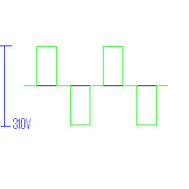
I have tried to boost my low-voltage (12V) PWM signal up to 600Vpp signal. Actually I couldnt get enough help from anywhere, anybody...
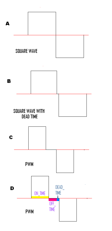
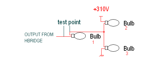
Anyway I have designed and Half bridge with driving Mosfets via IR2110. I read several papers with this usage... I want to ask that which is using to change duty cycle of the output signal? does it change by increasing/decreasing of dead-time or duty cycle? I am using a microcontroller and it generates two PWM signal which if HI is low, LI is high.

Thanks,
 

Dear sir,
would you check the attached file, it is a power module including a boost and an inverter. by the way, the duty cycle has a great influence on the output voltage.
 

Attachments

  • PN_solar200808.pdf
    127.6 KB · Views: 455

If you divide whole circuit into different sections according to functions, it will be lot more easy to end up with a working prototype. For example,
1. PWM signal generation.
2. Driver stage for output power switching devices.
3. Output stage
4. Voltage regulation.
5. Protection against overload etc.

For 12V operation it is better to use push-pull output stage not half bridge. This depends according to power requirments. You have to use a transformer to step up voltages. Either ferrite core for high frequency or iron core for low frequency.
 
Last edited:

Dear sir,
would you check the attached file, it is a power module including a boost and an inverter. by the way, the duty cycle has a great influence on the output voltage.

Hello,

I'm agree with you that the duty cycle has a great influence on the output signal. But what about the deadtime between two complementary PWM signal. I have changed only deadtime between PWM signals to change duty cycle of output stage.

thanks for your reply.

---------- Post added at 13:42 ---------- Previous post was at 13:34 ----------

If you divide whole circuit into different sections according to functions, it will be lot more easy to end up with a working prototype. For example,
1. PWM signal generation.
2. Driver stage for output power switching devices.
3. Output stage
4. Voltage regulation.
5. Protection against overload etc.

For 12V operation it is better to use push-pull output stage not half bridge. This depends according to power requirments. You have to use a transformer to step up voltages. Either ferrite core for high frequency or iron core for low frequency.

Dear ALERTLINKS,

you are absolutely right and the sections you mention must be designed step by step. İf I can explain my project step briefly:

1-) I generated Two PWM signals that if one of them is low, the other one is high. The same frequency, same amplitude,same duty cycle, but phase is different.
And of course, I've already added enough deadtime between these signals.
2-) For my driver stage, I want to use IR2110 N-Mosfet driver chip, so after a search, I choosed to design H-Bridge topology.
Here is my problem: I want to ask that which is using to change duty cycle of the output signal? does it change by increasing/decreasing of dead-time or duty cycle? I am using a microcontroller and it generates two PWM signal which if HI is low, LI is high.

By the way, if you have push- pull topology based on IR2110, can you share with me?

Thanks so much for your help.
 

The IR2110 already includes a deadtime between the HO and LO.
I have one solution for you, it may help you:
Look at circuit_1, the microcontroler produce two complementary pulses (50Hz) (RB1 and RB2, the PIC also generates one PWM (CCP1) (8KHz for example). The TC4469 is a MOSFETs drive for stepper motor but you can use it for your design. follow the circuit_1 and you will get the signals of circuit_2.
circuit_1.jpgCIRCUIT_2.jpg
 

These signals already include deadtime(through PIC16F877A), when you get these signals, try to introduce them to the IR2110 and your problem will be definitly solved. you may need only two signals, I do not know if you need 4. anyway, if two or four, the circuit give you up to four signals. but please let me know if your problem is solved.
I do not know if Mr. ALERTLINKS agrees with me or not, but I have implemented the hardware for this circuit and all is okay.
 

Unfortunately, I have to use IR2110 chip. I have tested my circuit again. Maybe my problem is not getting correct signal from HO and LO.
May I ask a question? Do HO and LO signals have to be overlapping?

---------- Post added 12-11-11 at 00:28 ---------- Previous post was 11-11-11 at 23:29 ----------

Here is my HO-Vs and LO-COM signal:

**broken link removed**

Here is my Vs-COM signal:

**broken link removed**


what is the problem on Vs signal?
 

Dear ultrasonic,
Please send me the circuit as it is implemented. I wonder if these signals are for the boost converter of for the half-bridge ?
IR2110 has to give you a signal HO-vs but when you put the oscilloscope probe to LO (oscilloscope ground not connected), you get signal.
 

Dear ultrasonic,
Please send me the circuit as it is implemented. I wonder if these signals are for the boost converter of for the half-bridge ?
IR2110 has to give you a signal HO-vs but when you put the oscilloscope probe to LO (oscilloscope ground not connected), you get signal.

Dear youcef here is my schematic:

**broken link removed**

I am using these topology to boost my signal up to 400-600Vpp.

thanks for your help.
 

C3, filter capacitor 2.2uF is of low value. Increase it to 330uF. It has to filter mains 50Hz from rectifier bridge. Otherwise circuit seems ok.
Dead time is of small duration( around 1uS to 4uS). The rest of period is controlled by pwm signal.
LO and HO signals seems ok showing some 40% duty cycle. What frequency is used? Vs is square wave, it should'nt be. It may be due to low value filter capacitor on mains, if it is 50 Hz. What is amplitude of this signal.
Check for IR2110 And FETs, if they are not damaged. There should be some output.
 
Last edited:

C3, filter capacitor 2.2uF is of low value. Increase it to 330uF. It has to filter mains 50Hz from rectifier bridge. Otherwise circuit seems ok.
Dead time is of small duration( around 1uS to 4uS). The rest of period is controlled by pwm signal.
LO and HO signals seems ok showing some 40% duty cycle. What frequency is used? Vs is square wave, it should'nt be. It may be due to low value filter capacitor on mains, if it is 50 Hz. What is amplitude of this signl.
Check for IR2110 And FETs, if they are not damaged. There should be some output.

Dear ALERTLINKS,

Thanks for clear help. I will change C3 filter capator as you said. And I also set deadtime around 1uS-4us. As you mentioned, duty cycle %40, frequency is 30khz. the circuit operates 25khz-38khz.

What do we expect Vs signal to be? I always get this square wave.

with kind regards,
 

You should expect signal like this of 35KHz if checked against common point of load connected 1/2 Vcc volts.
50_1321094793.png


But due to use of series capacitor in output and common poin connected to 0V, the potencial when both FETs are off (floating) will be different but should get voltage swing to full Vcc when Upper fet is on and 0V when lower fet is on.
 
Last edited:

You should expect signal like this of 35KHz if checked against 1/2 Vcc volts.
50_1321094793.png


But due to use of series capacitor in output, the potencial when both FETs are off (floating) will be different but voltage swing to full Vcc when Upper fet is on and 0V when lower fet is on.

I think I understand now, you mean that IR2110 invert LO signal and it adds HO and LO, then give the signal from Vs pin, right?

---------- Post added at 13:11 ---------- Previous post was at 13:00 ----------

C3, filter capacitor 2.2uF is of low value. Increase it to 330uF. It has to filter mains 50Hz from rectifier bridge. Otherwise circuit seems ok.
Dead time is of small duration( around 1uS to 4uS). The rest of period is controlled by pwm signal.
LO and HO signals seems ok showing some 40% duty cycle. What frequency is used? Vs is square wave, it should'nt be. It may be due to low value filter capacitor on mains, if it is 50 Hz. What is amplitude of this signal.
Check for IR2110 And FETs, if they are not damaged. There should be some output.

Dear ALERTLINKS,

When I tested my circuit I didnt add a load to the outout of my H-bridge, so does it also make problem not to see Vs signal in correct waveform?

Or we expect to see Vs signal like in your diagram despite not connecting a load?

thanks so much,
 

IR2110 swithes each Fet on and off seperately according to input. When lower fet is on center point is pulled towards 0V as source of lower fet is connected to 0V. when upper fet turns on, center point is pulled towards +Vcc as drain of this fet is connectd to +ve. It is obvious that if both fets are turned on simultaniously, it will cause a short circuit between +ve and -ve. Both fets will probably get destroyed. As fet takes around 1uS to switch off when input signal is turned off so is the need for dead time. It lets one fet to set completely off and after small time the other fet can be turned on.
What is value of voltage swing and frequecy is in output.
 
Last edited:

hello mr.alertlink and ultrasonic,
I enjoyed the discussion of you both people but as far as i concluded,the question of MR.ULTRASONIC is that how he can reduce/increase the duty cycle of his input squre wave generating by the micro-controller prior to feeding the high/low side ir2110 and then to half bridge.plz if u don't mind tell him and me also if you hve' some idea of this e.g 50% to 25% etc.regards

Dear ch wazir,

After spending lots of time, I can say that the output duty cycle is changed by increasing/decreasing of deadband time between two PWM signals.
 

After spending lots of time, I can say that the output duty cycle is changed by increasing/decreasing of deadband time between two PWM signals.

Consider a half cycle of a square wave,it has maximum duty cycle whitch is 50%. In this time period of half cycle we divide it in two portions ON_Time and OFF_Time. Now varying the value of these, we get PWM. It is called "pulse width modulation" becuse if you see waveform, the width of on time and off time varies. Next half cycle also have this relationship, then total time period and frequency remains same.
As off time and dead time mix with each other, your observation is right but technicaly they are different.
75_1321128534.png

pwm tutorials,
**broken link removed**


Detailed insight,
 
Last edited:
This waveform can be developed due to capcitative load. This capacitor loading could be even from oscilloscope leads. If a capacitor is on output it is charged when output is high, when fet is turned off, the capacitor retains charge aoutput shows full positine volts until lower fet turns on and capacitor is dicharged. But now when lower fet is turned off, capacitor remaind discharged showing 0v on output.It seems there is square wave on output. In actual use, PWM will work.
This circuit will help testig PWM and reading and viewing actual condition using three same tupe of small ac 220 volt bulbs

49_1321136434.png


Bulb2,3 are in series and connect to 310 volts. They will half lit equally. Their center point will be 155V. bulb1 is in series with center point output of hbridge. When switching tie of both feis equal it will be 50% voltage level , there be no current through bulb1. With change of current it will lit and luminance of bulb2,3 according to pwm applied. most important on bulb1 scope can be connected to see actual waveform.

Dear ALERTLINKS,

Thanks for all of your reply, they are all helpful for me. After you mentioned about capacitor loadind from the scope, I have tested my H-bridge circuit with changing dc supply to 12V and connecting a RC circuit to the output of my H-bridge, R simulates empedance of transformer. When I look at the scope, the waveform seems what we want to see. Here it is:
**broken link removed**

Now, I am sure that H-bridge circuit is also working well at 300V dc supply, but I think I must pay attention to choose Capacitor that is at the output of H-bridge and also empedance of power transformer. Even , I may think about enductance of the output load, because there will be a RLC circuit that can make very high voltages when my output drive (ultrasonic transducer) gets resonance frequency.

With kind regards,
 

Status
Not open for further replies.

Similar threads

Part and Inventory Search

Welcome to EDABoard.com

Sponsor

Back
Top