Continue to Site

Welcome to EDAboard.com

Welcome to our site! EDAboard.com is an international Electronics Discussion Forum focused on EDA software, circuits, schematics, books, theory, papers, asic, pld, 8051, DSP, Network, RF, Analog Design, PCB, Service Manuals... and a whole lot more! To participate you need to register. Registration is free. Click here to register now.

4-bit BCD Adder (Calculator Style)

Status
Not open for further replies.

arwayeyen

Junior Member level 3
Joined
Feb 27, 2012
Messages
31
Helped
0
Reputation
0
Reaction score
0
Trophy points
1,286
Activity points
1,484
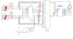
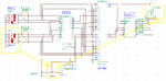
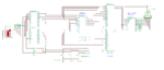
We are to design a calculator style adder on a breadboard with the following specifications:

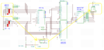
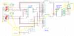
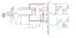
INPUT: One 4-bit BCD implemented by SPDT switches, 1 bit called 'PLUS' and 1 bit called 'EQU'
OUTPUT: 4-bit Sum

The process should work like an ordinary calculator. The output displays the first input. When PLUS is pressed, it is ready to accept the next input and the output will display the second input. When EQU is pressed, the output will display the sum of the two numbers.

If anyone could please help me out with this, provided with a logic diagram and an explanation of the circuit, that would be of huge help. :razz:
 

Update: Output is implemented via a a (1) 7 segment display.
 

:)
In theory for this project you may use one IC 4 bit binary full adder and one IC quadruple 3 lines to 1 line multiplexer. The result of the multiplexer to be applied to a BCD to 7 segment decoder and address multiplexing to be implemented with push buttons.
In practice we may use for example two IC dual 4-line to 1-line multiplexer (SN74153). The push buttons and some diodes must be connected generate the three needed addresses: 00, 01, 10.
MUX binary input address 00 = selection of A input
MUX binary input address 01 = selection of B input
MUX binary input address 10 = selection of result

4 bit binary full adder = SN7483
BCD to 7 segment decoder = SN7447

If none of the buttons pressed then the output of MUX= 0000.
See the diagram attached:
 

Attachments

  • SUM Project.png
    SUM Project.png
    127.4 KB · Views: 365
:)
In theory for this project you may use one IC 4 bit binary full adder and one IC quadruple 3 lines to 1 line multiplexer. The result of the multiplexer to be applied to a BCD to 7 segment decoder and address multiplexing to be implemented with push buttons.
In practice we may use for example two IC dual 4-line to 1-line multiplexer (SN74153). The push buttons and some diodes must be connected generate the three needed addresses: 00, 01, 10.
MUX binary input address 00 = selection of A input
MUX binary input address 01 = selection of B input
MUX binary input address 10 = selection of result

4 bit binary full adder = SN7483
BCD to 7 segment decoder = SN7447

If none of the buttons pressed then the output of MUX= 0000.
See the diagram attached:

You sir, you really are a life saver! One more, what are the value of those resistors and what diodes to use though?

Thank you so much!

---------- Post added at 14:43 ---------- Previous post was at 14:22 ----------

Oh, and why are they two 4-bit inputs? How does this work? Which one is the 'Plus' bit? Does this mean that when I press the A input and then press the B input, it will add internally? Then when I press the SUM, it will give an output of their sum?
 

Update: I've tested this out. The sum works great up until number 9. Problem is I can't get the B to display and the A is displayed on using the B switch.
 

No, this it’s a very simple circuit implementation allowing us to simulate the calculator summing function.
All calculations are performed instantaneously by the summing circuit at the time of setting A and B values.
If no buttons are pressed, the multiplexer address set by the pull-up resistors = 11, and we have selected C3 input for each multiplexer section ( now connected to GND) so the displayed result = 0.
Each time we press a button we changes the multiplexers address input.
As for example pressing the '' A INPUT '' button, the multiplexer address change to ''00'', multiplexer input set for C0 and the displayed number = input A
Pressing ''B INPUT'' (that’s the PLUS button ) generates the multiplexer address ='' 01'' and multiplexers input number to be set for C1 .
Pressing '' SUM RESULT'' button (that’s the EQU button) we generate an multiplexer address = '' 10'', inputs selected for C2, on the multiplexer output we get the SN7486 output.
 

Attachments

  • AINPUT_v1.png
    AINPUT_v1.png
    46.2 KB · Views: 145
  • BINPUT_v1.png
    BINPUT_v1.png
    39.8 KB · Views: 142
  • SUM A_B_v1.png
    SUM A_B_v1.png
    46.2 KB · Views: 128
I got the operation but can this be done using just one 4-bit BCD only?
 

Yes, that's possible. Need to add some latches for the A and B input data. See the attached diagram:
 

Attachments

  • LATCH_sum.png
    LATCH_sum.png
    172.3 KB · Views: 132

And by the way, for a complete arrangement need to change the SN7447 'BCD to 7 segment decoder' with 'hex to 7 segment decoder' like DM9368
**broken link removed**
 

Why does it need to have the hex to 7 segment? To output only from 0 to 9?
 

The DS9368 device accepts a 4-bit binary code and produces hexadecimal decode format which produces numeric codes ''0'' thru ''9'' and alpha codes ''A'' through'' F''.
So the new circuit accepts two 4-bit binary words to produce the hexadecimal output. In this case we need to add also a supplementary digit for the carry out...
 

Attachments

  • 2 digit sum.png
    2 digit sum.png
    224.4 KB · Views: 144
I only need 1 7 segment display sir.

---------- Post added at 20:48 ---------- Previous post was at 20:46 ----------

And how does this operate now?
 

No changes.
First set the switch to introduce the 'A' number.
Press the 'A INPUT’ button load the data into the latches and display the result on the 7 segment LEDs. Release the button.

Now reset the switches for the 'B' number.
Press the ‘B INPUT’ button to load the B number into the latches and display the number on the 7 segment LEDs. Release the button.


To obtain the final result press the ‘SUM RESULT’ button….
 

So, if say I make an input of 1 + 1, I'll just set the switch to 1 and press both the A input and B input and the sum would produce 2?

---------- Post added at 21:03 ---------- Previous post was at 21:02 ----------

Why do we need to add a supplementary digit for the carry out?
 

1. Yes.

2. Using a single digit we are limited to display up to binary 1111 = F hex, so that's the idea for the new attached diagram in post #11.
 

1. So what does it display on the second 7 segment?
2. What kind of IC are U8 and U10?

---------- Post added at 21:29 ---------- Previous post was at 21:27 ----------

3. Are pin2 and pin 14 connected together in the first MUX?
 

1. Need to consider we are able to set any binary number up to 1111 (F hex) for A and B inputs and the maximum result in this case up to 0001 1110 (1E hex)

2. U8/U10 that's a NOT gate, also called an inverter.

---------- Post added at 15:32 ---------- Previous post was at 15:31 ----------

3. No, that's a typo error. :-D
 

So you're saying that if only 1 7 segment display is used, the output is up until E only? And the function of the 2nd display is to raise the limit of output until F?

---------- Post added at 21:38 ---------- Previous post was at 21:35 ----------

2. What is the function of the 7475?
3. Can the Decoder be used in a common anode display?
 

No.
For A=(0 , F) and B = (0, F)
the final sum displayed sequence:
00
01
02
03
04
05
06
07
08
09
0A
0B
0C
0D
0E
0F
10
11
12
13
14
15
16
17
18
19
1A
1B
1C
1D
1E

---------- Post added at 15:44 ---------- Previous post was at 15:39 ----------

2. The SN7475 Series = Quadruple Bistable Latches
Used as temporary storage for the input binary information. Information present at a data D input is transferred to the Q output when the enable C is high and the Q output will follow the data input as long as the enable remains high. When the enable goes low, the information that was present at the data input at the time the transition occurred is retained at the Q output until the enable is permitted to go high.

---------- Post added at 15:47 ---------- Previous post was at 15:44 ----------

3. But that’s a common anode display mode, here the anodes of all the LEDs are joined together and the individual segments are illuminated by connecting to a low voltage.
 
Sorry for so many questions. I also need to explain the circuit properly while attempting this to work in a breadboard. Thank you so much for all your help. Really appreciated!

---------- Post added at 21:54 ---------- Previous post was at 21:52 ----------

What if I only want to add from 0 to 9?
 

Status
Not open for further replies.

Similar threads

Part and Inventory Search

Welcome to EDABoard.com

Sponsor

Back
Top