Welcome to our site! EDAboard.com is an international Electronics Discussion Forum focused on EDA software, circuits, schematics, books, theory, papers, asic, pld, 8051, DSP, Network, RF, Analog Design, PCB, Service Manuals... and a whole lot more! To participate you need to register. Registration is free. Click here to register now.
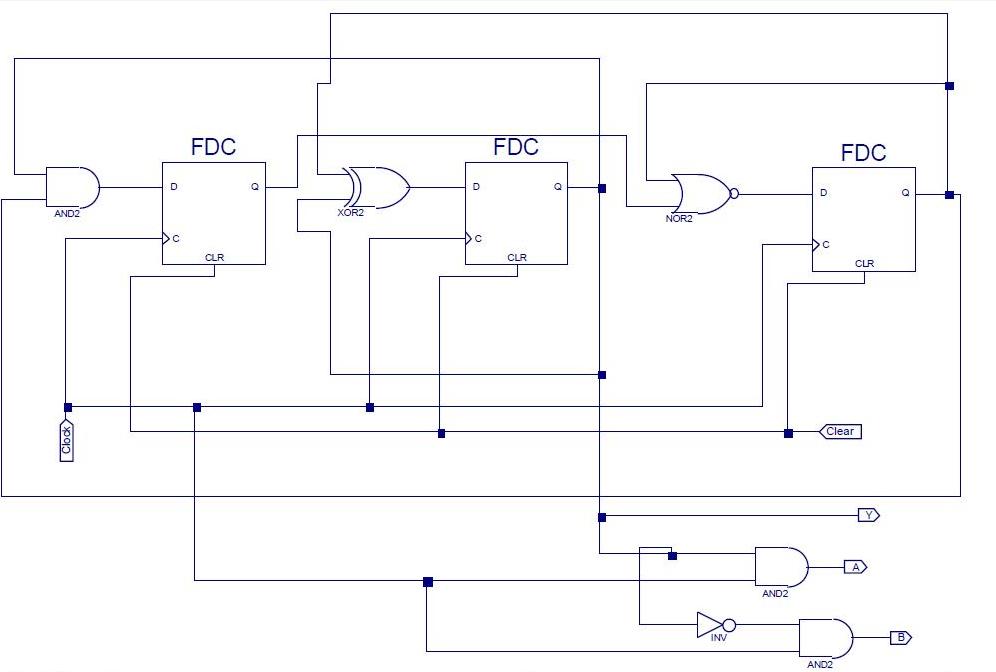
Hi... The idea is very simple... We need to have a mod 5 counter...
000
001
010
011
100
000
001
010
.
.
.
.
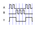
As you can see the middle bit has a period of 5 times the system clock... It is high for two clock cycles and low for three clock cycles. This is 'Y'.
To get 'A', I have connected 'Y' and system clock to an AND gate.. When 'Y' is high...The output will be the same as system clock....(you get two cycles).
To get 'B', I have connected 'Ycomplement' and system clock to another AND gate.. The output is 'B'... The output is same as system clock when the Y is low(you get three clock cycles)... And voila...
It really depends on whether all those signals are outputs or some are inputs. Convention would make A and B the inputs while Y would be an output. If that is the case a simple SR flip-flop is all you need. A rising edge on input A makes Y go high and a rising edge on input B makes it go low.
thanks all for the reply. what i exactly need is the one described by betwixt. Input A rising edge will make Y go high & input B rising edge will make Y go low.
This site uses cookies to help personalise content, tailor your experience and to keep you logged in if you register.
By continuing to use this site, you are consenting to our use of cookies.