Continue to Site

Welcome to EDAboard.com

Welcome to our site! EDAboard.com is an international Electronics Discussion Forum focused on EDA software, circuits, schematics, books, theory, papers, asic, pld, 8051, DSP, Network, RF, Analog Design, PCB, Service Manuals... and a whole lot more! To participate you need to register. Registration is free. Click here to register now.

A little confused on theory of decoupling capacitors

Status
Not open for further replies.

tasctasc

Member level 1
Joined
Jul 13, 2011
Messages
40
Helped
0
Reputation
0
Reaction score
0
Trophy points
1,286
Activity points
1,589
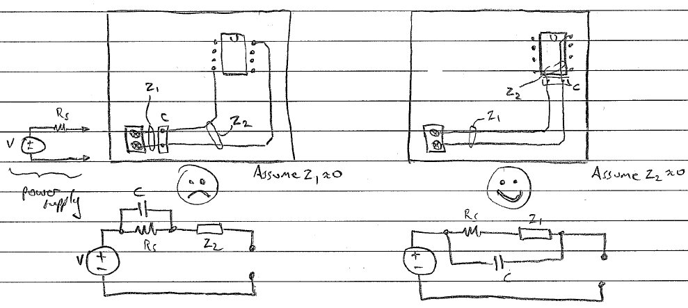
I am a little confused as to the theory of decoupling capacitors. I understand that they provide the immediate charge requirements when there is a voltage drop due to dI/dt or IR noise, since the decaps are charged up and when there is a voltage drop they essentially share their charge with the corresponding circuitry. However, considering the frequency domain, the decaps act as a bypass to high frequency noise on the supply and essentially shunt this noise. Are these two distinct noise suppression mechanisms taking place simultaneously or are they one and the same thing? Some papers seem to say these two things are two distinct mechanisms and both contribute to suppression, but most papers only mention one of the two mechanisms. Is someone able to explain exactly what mechanism is causing the noise suppression?
Many thanks.
 

Yes, you're right - it is one and the same thing. Rather than trying to treat their 'transient' (time domain) and 'noise' (frequency domain) characteristics seperately though, they can be unified by the following picture:

The power supply feeding (powering) the circuit can be well described as an ideal voltage source in series with a small, but finite impedance. The voltage source represents the regulated supply voltage, and the impedance consists of both a resistive component (describing the effect of ohmic interconnection losses as well as the regulator output resistance) and a reactive component describing the inductance of the physical connections. This model can actually be extended to EVERY supply node of the circuit, since each interconnected node will have it's own unique conductive path linking itself to the supply.

It is the series impedance responsible for the voltage drops observed with current - the resistive component results in IR loss, and the inductive component gives rise to transient dI/dt drops. Decoupling capacitors are placed in SHUNT with the supply within a circuit, thereby appearing in PARALLEL with the aforementioned impedance. This serves to DECREASE the effective supply impedance for all frequencies > 0. That's right - they can't improve the DC (resistive IR) losses within a circuit, but they diminish the magnitude of transient (which by definition, has frequency components > 0) voltage drops.

This model also illustrates why it's crucial (for effective decoupling) to have the capacitors right AT the power supply pins of the part being decoupled, as any series resistance between the capacitor and the device being powered is not shunted by the capacitor's own reactance (and therefore isn't "compensated for"). It also shows why high frequency circuits have multiple decoupling capacitors of different values in parallel - sadly, a real capacitor is far from ideal and has internal inductance (and resistance). At high frequencies, these parasitic effects serve to RAISE the impedance of the capacitor, preventing it from performing the desired decoupling task. By having a (typically smaller) valued capacitor in parallel, it can be arranged that when one capacitor becomes ineffective (for frequencies > self resonance) the second (3rd, 4th...) capacitor is below self resonance (and still behaving as an intended shunt capacitive element).

Please don't primarily view the problem as one of 'noise suppression' as this approach is misleading. By considering the equivalent circuit of each interconnection, however, the mechanism by which the decoupling capacitors serve to suppress 'noise' (by the formation of low impedance voltage divider networks) can be readily visualised.

I hope that helps - decoupling caps are wonderful things! :)
 
Thank you so much for your detailed and helpful response, thylacine1975.

Are you able to explain a bit more what is meant by "it's crucial (for effective decoupling) to have the capacitors right AT the power supply pins of the part being decoupled, as any series resistance between the capacitor and the device being powered is not shunted by the capacitor's own reactance (and therefore isn't "compensated for")? I thought decaps should be placed as close as possible to the circuits being powered to be most effective since any extra resistance between the decap and the circuit serves to increase the overall effective impedance of the decap?

Also, with this way of visualizing the decap behaviour, is it possible/easy to approximate the voltage drop obtained? Since the impedance is stated in the s domain, is it correct that to approximate the noise one would have to feed the model a sinusoidal waveform of single frequency to find the 'noise'? However, the switching current pattern of transistors couldn't be further from a sinusoid ;o) Do you have any suggestions on how to estimate the noise given the various impedances and an approximately triangular periodic waveform? Most papers use charge sharing, however, make the assumption that all the immediate current requirements come from the decap with no current at all coming from the voltage source. Is this a fair assumption?

Thank you again for your pearls of information :eek:)
 

Yes that's a very good explanation by thylacine1975.

I think it's easiest to see capacitors as small energy reservoirs, that try to keep voltage at their terminals constant. When for example an IC switches outputs, there's short but large fluctuations in current consumption. The wiring /circuit board traces between power supply and that IC makes those current fluctuations cause local voltage fluctuations (how much, depends on wiring resistance / induction, frequency & magnitude of the current fluctuations).

With no decoupling capacitors in place, those voltage fluctuations might be large. But with a decoupling capacitor in place, the capacitor either supplies (when voltage goes down) or consumes current (when voltage goes up), and by doing so causes the voltage fluctuations to become smaller.

A small capacitor (like those typical 100 nF ceramic) reponds very fast, but has small capacity, so it's good at supplying current for very short periods (like the current fluctuations you get when fast digital logic switches outputs). But because of that high-frequency behaviour, it needs to be very close to the point where those current fluctuations originate, to do its job effectively. Like directly across GND/Vcc supply pins of that logic IC.

A large capacitor (like the electrolytic ones you find inside power supplies) has much larger capacity, but in comparison lousy high-frequency response. So it would do nothing to counter high-frequency current fluctuations. That's why you tend to find these capacitors at board power supply entry points, or scattered in a few places across a board - they deal with low-frequency, high-current power fluctuations.

So effective decoupling uses as combination of different capacitor types in parallel, location & types depending on application. As for exact numbers, you'd have to know frequency & magnitude of the current transients, the exact characteristics of board traces, impedance vs. frequency of the capacitors used, etc etc. Not impossible, but in a way a kind of black art... ;-)

Most papers use charge sharing, however, make the assumption that all the immediate current requirements come from the decap with no current at all coming from the voltage source. Is this a fair assumption?
Yes, for high-frequency current transients, that sounds a reasonable assumption. Hence the problems you might have when you have such high-frequency current transients, but no decoupling capacitors in place. Although small in size, their local effect can be extremely important.
 
Last edited:
All they are for, is making an AC short circuit for transient current.
Because you have to assume that your upstream power source
is pretty much inductive and can't help you until too late for the
switching event in question.

Of course just like cops and hookers, you can never find a short
circuit when you really need one. Only a reasonable approximation.
 

There are decoupling capacitors and bypass capacitors. Their roles are different although people lump them together. Maybe that is the two things that you are referring to? Bypass caps provide a low impedance path as you mentioned, mostly to reduce supply spikes from finite source impedance. If only bypassing is used, all circuits share a single bypass cap. If one circuit spikes the supply all circuits will see it, i.e. they are coupled via the power supply.

Decoupling caps also provide this path, but they mainly "decouple" circuits from each other. Each circuit will have its own decoupling capacitor and there will be a small resistor to isolate the circuits from each other. That way a current spike from one circuit won't spike the supply to another circuit.

rg

---------- Post added at 18:30 ---------- Previous post was at 18:25 ----------

Also, with this way of visualizing the decap behaviour, is it possible/easy to approximate the voltage drop obtained? Since the impedance is stated in the s domain, is it correct that to approximate the noise one would have to feed the model a sinusoidal waveform of single frequency to find the 'noise'? However, the switching current pattern of transistors couldn't be further from a sinusoid ;o) Do you have any suggestions on how to estimate the noise given the various impedances and an approximately triangular periodic waveform?

If you find the s-domain impedance you can find the response to any type of current spike using Laplace transforms. V(s) = I(s)*Z(s). Then take the inverse Laplace of V(s) to find the time domain response.
 

Hi again all - and thanks for everyone's extra perspectives!

Tasctasc: Just to clarify what I'd meant by my wordy statement "it's crucial (for effective decoupling) ...". Yes, your thought IS correct, and this is what I was (poorly) trying to articulate! Decaps go right next to the "device being powered" (what I meant when I said "part being decoupled"). I think the following sketch shows we're on the same page:


RobG - I'd never actually considered the distinction between their decoupling and bypass roles before. Hmm. Good point though. I guess the distinction blurs when you don't explicitly add (interstage) resistors, yet one still retains the benfit of some isolation afforded by the interconnection impedances.

In terms of predicting the voltage drops ('noise') arising from repetitive, triangular current waveforms, yes you could certainly use Laplace techniques. Alternatively, estimating the magnitude of the voltage drop across the wiring inductance (L) via V_drop = L di/dt, where di/dt is the slope of the triangular current profile would be a reasonable first order approximation. I've attached an excerpt from a brilliant (and very easy-to-read) text that covers a lot of what we've discussed from the perspectives of TTL logic power distribution design of 30+ years ago. The book is "Digital Hardware Design" by Ivor Catt, David Walton and Malcolm Davidson, published by MacMillan Press in 1979. (I'll assume this snippet falls under the copyright definition of "fair use"... enjoy!)
 

Attachments

  • Catt.pdf
    361.5 KB · Views: 135
Status
Not open for further replies.

Part and Inventory Search

Welcome to EDABoard.com

Sponsor

Back
Top