Welcome to our site! EDAboard.com is an international Electronics Discussion Forum focused on EDA software, circuits, schematics, books, theory, papers, asic, pld, 8051, DSP, Network, RF, Analog Design, PCB, Service Manuals... and a whole lot more! To participate you need to register. Registration is free. Click here to register now.
if Vds is close to zero , means the device is in'linear resistance region'.
for digital circuits we make this to happen for output Vds to close to zero.
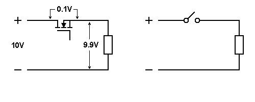
I suppose you mean Vds when the transistor is in the ON condition. If that's so, the reason is that Vds multiplied by Id represents a loss. Look at the schematic and think of the MOSFET as the equivalent of the conventional switch. If the MOSFET has a drop of 0.1V when it is in the ON condition, the load receives only 9.9V.
It's not only that the load does not receive the full voltage. The voltage drop in the transistor multiplied by the current becomes power that is uselessly turned into heat inside the transistor. Therefore, the closer Vds is to 0 in the ON condition, the better.
Firstly, Nmos is ON when Vgate = high, and Pmos is ON when Vgate = low. Also with the threshold voltage, and base on conducting condition, we can see that nMOS switch is "weak" 1, and pMOS is "weak" 0.
Secondly, For Nmos switch, source is typically tied to ground and is used to pull-down signals, and for pMOS switch,source is typically tied to Vdd, used to pull signal up. And note that the MOS transistor is a symmetric device, this means that the drain and the source terminal are interchangeable. For a conducting nMOS transistor, Vds > 0V; for the pMOS transistor Vds < 0V (or Vsd >0V). :smile:
This site uses cookies to help personalise content, tailor your experience and to keep you logged in if you register.
By continuing to use this site, you are consenting to our use of cookies.