Continue to Site

Welcome to EDAboard.com

Welcome to our site! EDAboard.com is an international Electronics Discussion Forum focused on EDA software, circuits, schematics, books, theory, papers, asic, pld, 8051, DSP, Network, RF, Analog Design, PCB, Service Manuals... and a whole lot more! To participate you need to register. Registration is free. Click here to register now.

[SOLVED] Schematic Vs Parasitic Layout delay times.

Status
Not open for further replies.

jgk2004

Full Member level 5
Joined
Dec 1, 2009
Messages
274
Helped
77
Reputation
154
Reaction score
74
Trophy points
1,308
Location
Munich Germany
Activity points
3,520
Hello all

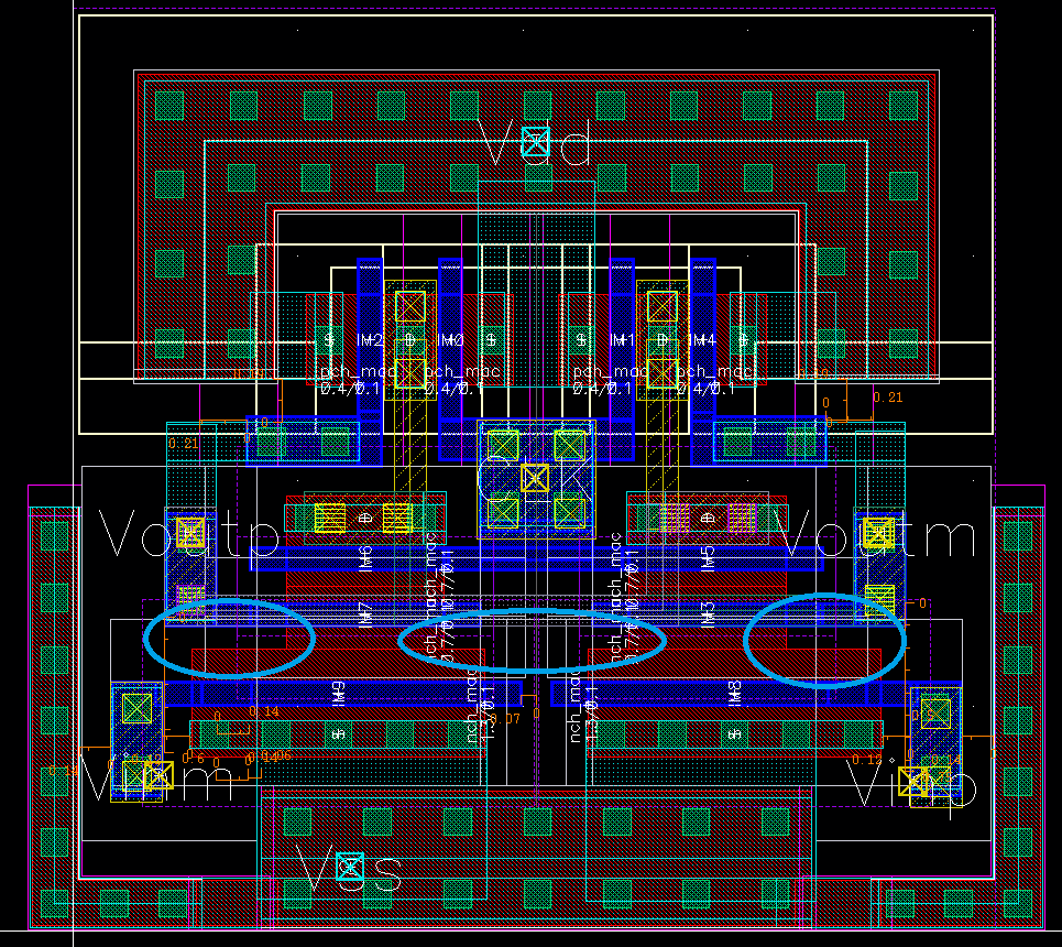
I am designing in 90nm CMOS and i need to keep delays to a minimum. I am designing a 4bit flash and after layout my delay times of each bit increase by from 210pS to350pS which is to much for my clock speed. My question is.. is my layout just bad or is this normal? How much of an increase from schematic to parasitic extracted would you expect... ?

Any help would be great

Jgk
 

It should not change more than 10% as a considerable variation. You need to look at the layout offcourse.
 

    V

    Points: 2
    Helpful Answer Positive Rating
So 10% is normal.. Would you recommend using minimum wire widths within this area? to minimumize added cap or should i be worried about series resistance? my min wire width is .12um, I have always been using .14 to .16.

Jgk
 

Both matters, but first concern is Series routing res. Just reduce the routing wire length in lower metals.
 

Ok sounds good. Just one last thing. For high speed designs in a 9 metal process, do most people use met 3 and up to reduce the cap to sub or is met 2 fine. I almost never use Met1 and use Met2 instead but maybe I should go to met3... Any advice?

Jgk
 

Ok sounds good. Just one last thing. For high speed designs in a 9 metal process, do most people use met 3 and up to reduce the cap to sub or is met 2 fine. I almost never use Met1 and use Met2 instead but maybe I should go to met3... Any advice?
Jgk
Both metals may be used. ( I like to add higher metals are useful for high current driving and low IR drops).
Your concern was speed. Stick to metal 2/3 and try to take help from schematic designer for margin :).
 
  • Like
Reactions: jgk2004

    jgk2004

    Points: 2
    Helpful Answer Positive Rating
Hello Varunkant2k,

Ok so I have got the layout delay down to 290ps, so now I'm only 80ps off, but this is still not 10%. I am no longer in Met 1 except at contact and I am routing in Met 3 and higher. I just don't think it is possible to reach a 10%. Have you every made a sense amp, since this is basically what a flash is made out of... just 15 of them.. What type of delays after layout would you except for a sense amp structure?

Thanks for the help
Jgk

---------- Post added at 14:14 ---------- Previous post was at 14:09 ----------

Also I have attached a picture of my core layout. I have one last question and that is. is it a bad thing to have the OD of three transistors not aligning properly? Would you recommend NOT doing this or is it OK? It is completely DRC clean, so i would think it is ok......


Jgk
 

It is not a bad thing to have OD of the three transistor align properly but I would avoid it especially if is high speed design. looking at your layout I think you might be able to break M9/M8 to have number of gates as 2 instead of 1, they will nearly line up with other devices M6/M7.

also are u connecting M6/M5 - M0/M1 with poly (not quite clear poly and metal 3 are both blue), this might be bad as poly has larger resistance and more parasitic cap. extract the layout and parasitics should give you an idea where you can better optimize, you can also have metal2 running underneath metal3 adding more parallel connection and reducing resistance.
 
  • Like
Reactions: jgk2004

    jgk2004

    Points: 2
    Helpful Answer Positive Rating
Hi Steadymind,

Thanks for the feedback. Just to answer your questions . Yes M6/m5/m0/m1 are all connected i poly but they all share the same 4pin contact. This is the best I can do.. If i route up into Met2 I would just open up the spacing.. so I would think the way I have it is best. As for your comment on taking the input transistors and having 2 gates instead of one. If I do this I will not be able to share the OD and thus would have metal contracts in there. Would you really think this is faster and better then what I have now? I just really like this compact layout, but if you really won't recommend the non-aligned OD i will do 2 gate input transistors.

Thanks for the feedback
Jgk
 

your points are valid. i just gave you alternate suggestions. get an extracted parasitic report, it will give an indication of where your delay is getting affected.
 
  • Like
Reactions: jgk2004

    jgk2004

    Points: 2
    Helpful Answer Positive Rating
My report says its only 2fF on the outputs. It was around 3.5fF so I have cut it back. I am just alittle worried of the uneven OD now. I think I will make another core with 2 gate inputs and see if the speed stays the same or becomes faster.

Thanks for the feedback
Jgk
 

A change from 3.5fF to 2fF decreased your delay from 350pS to 290pS. This seems very strange, I would be very cautious on this one. Is there any big change on extracted resistance ?
 

Sorry for the late reply, The reason why my time decreases is also since i increased the width of the input transistors to make the circuit overall much faster. I have also just added fingers, like suggested, to the input to have them align alot better and have thus got my delay down to 10%. Sorry for the confusion. I think overall, my starting circuit just needed a better prediction of the parasitics, and if so i could have been more accurate with designing my inputs to drive such a load.

Thanks all for the help
jgk
 

good to hear that you got your delay down. just out of curiosity did the OD sharing make a difference in parasitics compared to a device with 2 fingers?
 

Yeah it did but it wasn't the node affecting the speed. When sharing the OD the Parasitic was 30aF When having fingers and wiring up to met2 to connect it became 773aF.
Jgk
 

Status
Not open for further replies.

Part and Inventory Search

Welcome to EDABoard.com

Sponsor

Back
Top