Continue to Site

Welcome to EDAboard.com

Welcome to our site! EDAboard.com is an international Electronics Discussion Forum focused on EDA software, circuits, schematics, books, theory, papers, asic, pld, 8051, DSP, Network, RF, Analog Design, PCB, Service Manuals... and a whole lot more! To participate you need to register. Registration is free. Click here to register now.

PLL phase noise changing with reference divider

Status
Not open for further replies.

mtwieg

Advanced Member level 6
Joined
Jan 20, 2011
Messages
3,835
Helped
1,310
Reputation
2,626
Reaction score
1,405
Trophy points
1,393
Activity points
29,374
Hello,

First of all, I can't state the application in detail (it's ongoing research), but I think I can describe the system in enough detail. I'm asking this on behalf of a friend who has been fighting this issue for a while. Neither of us are experts on PLLs or phase noise, so we're looking for advice.

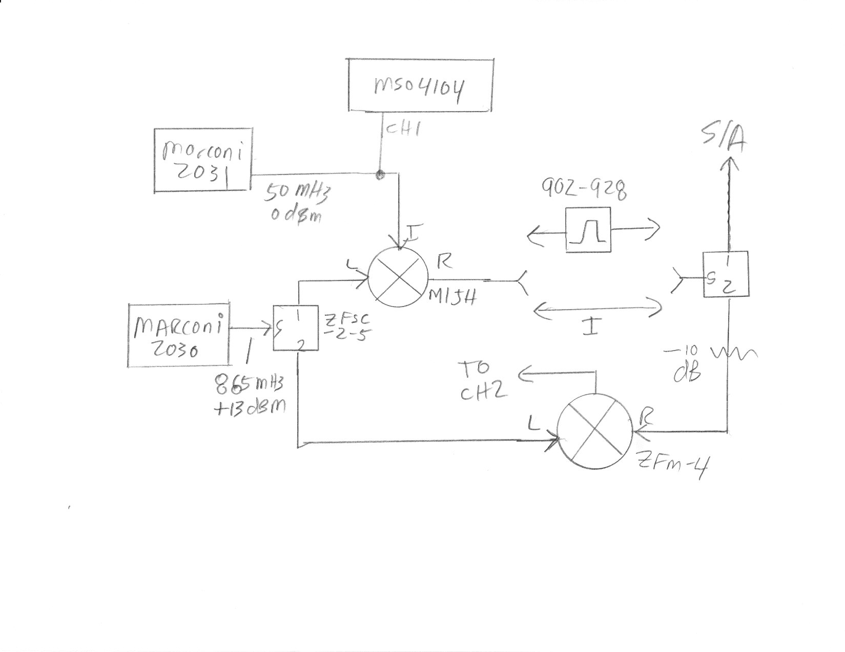
Basically we're trying to upconvert (to around 950MHz) a narrowband (about 50MHz, BW is about 500KHz) signal and transmit it wirelessly (SSB) to a receiver, which downconverts it back to the original 50MHz signal with as little error as possible. To generate the carriers on the receiver and transmitter sides he is using a combination of a ADF4111 PLL and a MAX2623 VCO. A 5MHz reference is connected to both sides via a coax cable. A block diagram is shown below.
mattsystem1.PNG

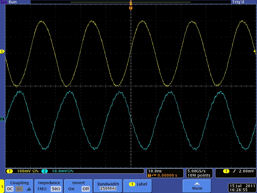
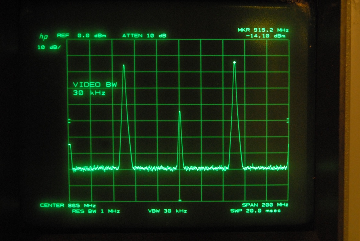
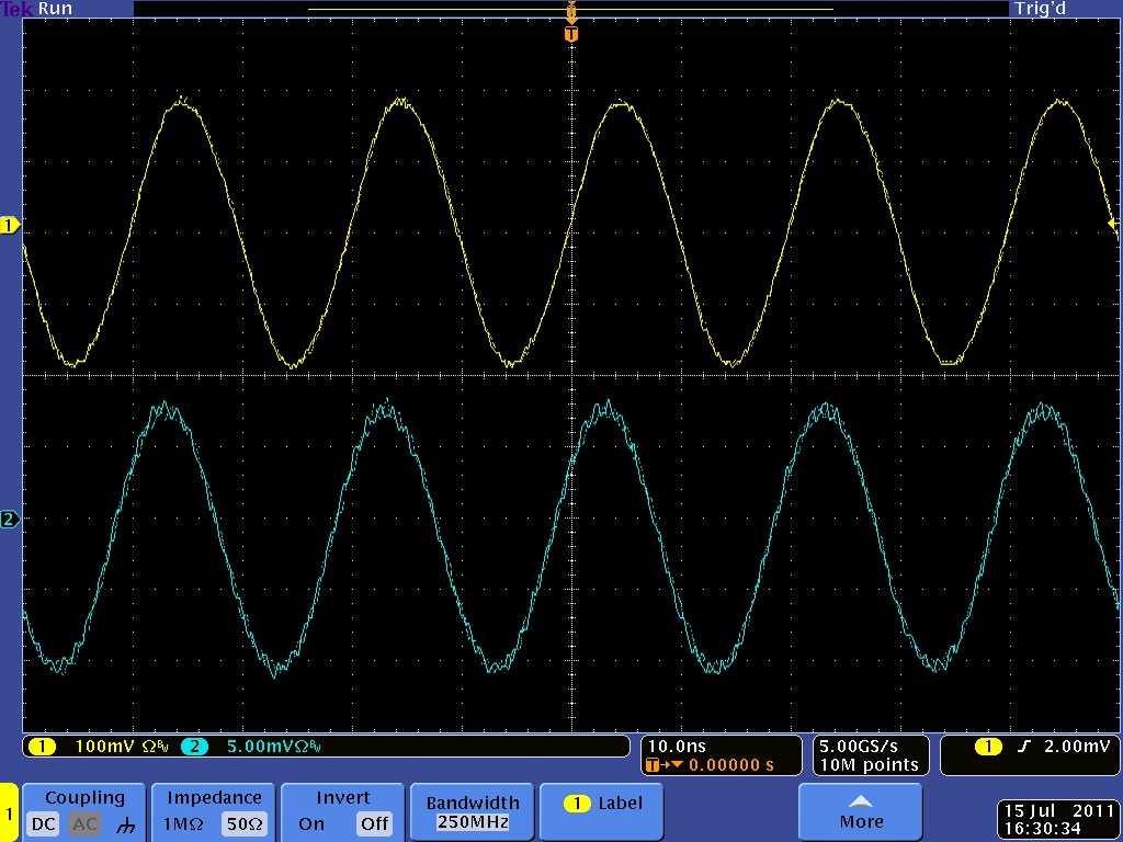
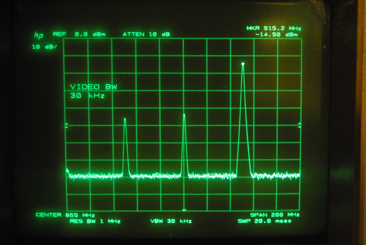
Everything looks fine on the bench (as shown by our spectrum analyzer). We can see the signal reproduced accurately over the whole system. However, when we use it to transmit actual data, we are sometimes observing artifacts that seem to be due to low frequency phase drift/error in the downconverted signal. After messing around with the system a lot, he found that these artifacts only appear when the PLLs are set such that the output of the VCO is not an integer multiple of the 5MHz reference (produced by a 10MHz oscillator with its output divided by a flip flop). The PLL has an internal reference divider (R counter) so that frequency resolution can be smaller than that of the 5MHz reference, which he desires. At first he was dividing it down to 200KHz internally (R=25), then multiplied it by N=~4750 to get around 950MHz. He would get noise results unless the the carrier was a multiple of 5MHz (N was a multiple of 25).

Even stranger, we tried a 10MHz reference in as well, and we saw the same thing. Like if we use a 5MHz with R=1 and N=181 to get 905MHz, it will give good outputs. But if we use 10MHz with R=2 and N=181 to get 905MHz, we will get noisy output. But then if we use fr=10MHz, R=2, N=180 to get 900MHz, it will work well again. This is really perplexing, since internally the divided reference should be exactly the same signal in all of these cases. But somehow these different settings get different results.

Has anyone ever encountered an issue like this? We've tested this exhaustively, and the problem is very consistent. The frustrating part is we can only observe this when doing a real experiment and reconstructing real data. When looking at noise on the signal analyzer, everything looks the same, despite getting different results from the experiment. Maybe we're not using the signal analyzer correctly...?

Thanks,
-Mike
 

Do you really mean you are transmitting it SSB? SSB means you are stripping off the carrier, and the phase/frequency information of the wireless signal no longer is fixed. It works fine for audio where you can stand big amounts of distortion and still understand the spoken words, but may be useless in other applications.

Are you sending the reference frequency to the fartheset receiver with enough amplitude that the input divider can reliably receive it without phase slips?

Try replacing your modulated 50 mhz tone with an unmodulated clean 50 mhz sine wave, send it wirelessly, and compare the received tone to the transmitted tone on an oscilloscope, and tell me what you see. Are they both clean sine waves with a fixed phase offset, or is one "walking" in phase with respect to the transmitted one? Are there other distortions on the received 50 mhz sine tone?
 
  • Like
Reactions: mtwieg

    mtwieg

    Points: 2
    Helpful Answer Positive Rating
Do you really mean you are transmitting it SSB? SSB means you are stripping off the carrier, and the phase/frequency information of the wireless signal no longer is fixed. It works fine for audio where you can stand big amounts of distortion and still understand the spoken words, but may be useless in other applications.

Are you sending the reference frequency to the fartheset receiver with enough amplitude that the input divider can reliably receive it without phase slips?
The reference frequency is exactly the same for the transmitter and receiver. It's literally the same signal, routed via coax. So it should essentially be coherent demodulation, except that the pll/vcos may act differently.

The distance between receiver and transmitter is less than a meter as of now. And the reference is buffered by op amps on both sides. So I don't think amplitude is a problem.
Try replacing your modulated 50 mhz tone with an unmodulated clean 50 mhz sine wave, send it wirelessly, and compare the received tone to the transmitted tone on an oscilloscope, and tell me what you see. Are they both clean sine waves with a fixed phase offset, or is one "walking" in phase with respect to the transmitted one? Are there other distortions on the received 50 mhz sine tone?
It doesn't "walk" (and it shouldn't, since they share a reference) but there is some phase jitter, which is expected. However if I recall correctly, changing the R and N values as I described doesn't noticeably change the amount of jitter. That's what I'm most concerned about.
 
Last edited:

I do not believe it. If it were a true homodyne system you would not be having these problems. You need to figure out what is going on. The best way is to actually compare the input and output signal unmodulated, either on a dual channel scope or on a baseband noise measurement system. Until you do the test, your assumptions are under question.

What IS the modulation? If it is ssb, there is your answer.

How are you using those mixers? When you upconvert, you have a RF + LO, and LO, and a LO-RF signal. You show a LPF, but which of those three outputs is getting thru to the receiver mixer?
 

I do not believe it. If it were a true homodyne system you would not be having these problems. You need to figure out what is going on. The best way is to actually compare the input and output signal unmodulated, either on a dual channel scope or on a baseband noise measurement system. Until you do the test, your assumptions are under question.
Right, if it really were coherent, then we shouldn't have any issues, but it's not quite coherent because the reference is being converted into two different carriers by different PLL/VCOs. So any phase noise between the two carriers will cause phase noise on the downconverted output.

What IS the modulation? If it is ssb, there is your answer.

How are you using those mixers? When you upconvert, you have a RF + LO, and LO, and a LO-RF signal. You show a LPF, but which of those three outputs is getting thru to the receiver mixer?
It's definitely SSB. After upconversion, the carrier and USB are filtered off with a LPF. The USB is attenuated by about -30dB and the carrier is down by about -15dB. Not great, but enough that it should behave as SSB should. On the downconverter side, there is a narrow 50MHz bandpass filter (not a LPF, my bad) after the downconverter.

So I'm pretty sure the PLL/VCOs are a source of noise, and that's not surprising. What I'm more concerned about is why certain settings on the PLL cause the noise to become worse.
 

Hi Mike,

Is it possible to include a sort of a maximum gain locked loop?
The variable would be the phase of the generated local carrier (a signal derived from the VCO output) for the synchronous demodulation.
But here the ideal signal error is not easy to generate since it is a function of the derivative of the demodulated signal amplitude (or power). And... the output amplitude may vary not because of the carrier phase only.

I think there must be a topology that helps maintaining the phase of the local carrier between +/- 45 deg in the least if the received signal (informative) has no silent intervals as in normal speech.

Kerim

Edited:
The phase correction of the carrier (taken from an output) is independent of the main PLL.
 
Last edited:

Hi Mike,

Is it possible to include a sort of a maximum gain locked loop?
Do you mean this as a modification to the PLL generating the carrier, or using a PLL as a detector?
The variable would be the phase of the generated local carrier (a signal derived from the VCO output) for the synchronous demodulation.
But here the ideal signal error is not easy to generate since it is a function of the derivative of the demodulated signal amplitude (or power). And... the output amplitude may vary not because of the carrier phase only.

I think there must be a topology that helps maintaining the phase of the local carrier between +/- 45 deg in the least if the received signal (informative) has no silent intervals as in normal speech.
Are you talking about carrier recovery from the SSB received signal? How could such a thing be better than the current setup, where the only noise comes from the inherent noise of the PLL+VCO?

I think you're talking over my head a bit...
 

1. Maybe its the interferes between two VCO through Ref TCXO. SO you can try add LC Pi filter on each branch of the ref signal. And the ref should be AC coupled.
2. You can use software ADISimPLL to simulated your TX VCO and RX VCO. You can set params to get opt phasejitter. Every time you change Ref divider N, etc, of the PLL, the PLL components should be changed to get phase margin not too bigger and not too smaller.
 
  • Like
Reactions: mtwieg

    mtwieg

    Points: 2
    Helpful Answer Positive Rating
I am very sorry, Mike... it seems I was confused when trying to find a solution. I forgot it is about a SSB link hence the local carrier phase won't affect by itself the output amplitude.
 

upconverting a signal with an LO, and filtering off one of the two sidebands is NOT called SSB!
 

1. Maybe its the interferes between two VCO through Ref TCXO. SO you can try add LC Pi filter on each branch of the ref signal. And the ref should be AC coupled.
So you mean the VCOs on the receiver and transmitter might be interfering with each other through the reference clock? Or interference from the 900MHz getting back into the reference on each one? The first one sounds improbably (since the reference is buffered at each point), but the latter is definitely a possibility, once which he's given thought to. In fact, it is the only reasonable explanation I could think of for the strange behavior (the situation I mentioned where using a 5MHz clock with R=1 and N=181 works, but 10MHz with R=2 and N=181 does not). Would this be caused by interference at the ref input (outside the ADF4111) or at the output of the R divider (internal to the ADF4111)?
2. You can use software ADISimPLL to simulated your TX VCO and RX VCO. You can set params to get opt phasejitter. Every time you change Ref divider N, etc, of the PLL, the PLL components should be changed to get phase margin not too bigger and not too smaller.
Yeah, I've been advising him that getting optimal noise will be a matter of compensating the loop response, but that doesn't explain the issues with the divider settings. If we think it's interference from the VCO output, is that something we could model in ADIsimPLL?

---------- Post added at 08:42 ---------- Previous post was at 08:38 ----------

upconverting a signal with an LO, and filtering off one of the two sidebands is NOT called SSB!
Oh? How so? I've been taught that eliminating the carrier and one sideband results in SSB, regardless of how the carrier and sideband are eliminated.
 

You are going to have to explain your signal you are trying to send in more detail for us to help
No problem. If anything is unclear just ask. We're pretty determined to solve this issue, so we're willing to go in depth. However we can't really reveal the application, since he's trying to get a paper published on it very soon. So I hope you'll understand if I can't get too explicit with the nature of the signal and its origin.

Here is a capture of the upconverted spectrum, after the LPF, before the antenna. It's centered around the carrier frequency. Note that this is with no actual 50MHz signal being put in; the two sidebands at +/-50MHz are just noise from a 50ohm source (this plot was gathered specifically for evaluating noise). So the actual signal will be much narrower in bandwidth than those lobes are, and higher in power. So you can see the LSB is passed while the USB is suppressed by >20dB. The carrier is about even with the LSB (it's higher before the LPF). You can also see the noise profile around the carrier from the VCO and PLL. We can't see any real change in it when changing the PLL settings.
SSBout.png
Right and it says:
One method of producing an SSB signal is to remove one of the sidebands via filtering, leaving only either the upper sideband (USB), the sideband with the higher frequency, or less commonly the lower sideband (LSB), the sideband with the lower frequency.
So that's what we're doing. Out of curiosity, why would one prefer the USB over the LSB?

Thanks,
-Mike
 

Mike

I've followed the discussion do far, the spectrum you're showing seems very very noisy and I don't understand why.

It seems noise comes from the baseband signal and is upconverted as LO is quite clean, but this is not possible if only a 50 Ohm noisy resistor is connected. Noise is white, why there is such a shaping around 60MHz and why is so high?

What do you really connect to the baseband port of the mixer?

Mazz
 

One option is to use a IQ Modulator as a single sideband mixer on the transmitter side, such as the Hittite HMC495. This would allow you to reject the carrier and the unwanted sideband with at least >40dB, which i dont think you are getting with a low pass filter since the unwanted terms are only 50MHz apart.
 
  • Like
Reactions: mtwieg

    mtwieg

    Points: 2
    Helpful Answer Positive Rating
Mike

I've followed the discussion do far, the spectrum you're showing seems very very noisy and I don't understand why.

It seems noise comes from the baseband signal and is upconverted as LO is quite clean, but this is not possible if only a 50 Ohm noisy resistor is connected. Noise is white, why there is such a shaping around 60MHz and why is so high?

What do you really connect to the baseband port of the mixer?

Mazz
Mazz,
There is a narrowband LNA between the 50 ohm source and the mixer. The noise level, and the shape of the noise spectrum (that V shape), are characteristic of the LNA we're using, so there's nothing surprising to us about the noise there. We've actually just verified that the overall noise figure of the entire system is less than 1dB (including the preamp, upconversion, wireless channel, and downconversion).

edit: actually, even after that explanation, you'll probably thing it's too noisy, which is understandable... that plot wasn't taken with a normal 50ohm terminator, but rather the actual signal source which picks up a lot of interference. With a 50 ohm terminator it is far cleaner. You'll just have to trust me when I say that the noise performance of the LNA+mixer is good. Believe me, he's spent nearly the past month measuring it.

---------- Post added at 08:00 ---------- Previous post was at 07:46 ----------

[/COLOR]
One option is to use a IQ Modulator as a single sideband mixer on the transmitter side, such as the Hittite HMC495. This would allow you to reject the carrier and the unwanted sideband with at least >40dB, which i dont think you are getting with a low pass filter since the unwanted terms are only 50MHz apart.
Yes, using something like that would probably help with the carrier and sideband suppression. Are you describing what wikipedia refers to as a Hartley modulator? The HMC495 has a quadrature splitter in the LO input, but I would also need to generate IQ versions of the baseband, correct?

Your idea is interesting, but do you expect that the problems we're seeing have to do with the upconversion/downconversion? I was expecting that it had something more to do with an oddity in the PLL or VCO themselves...
 

No Note that this is with no actual 50MHz signal being put in; the two sidebands at +/-50MHz are just noise from a 50ohm source (this plot was gathered specifically for evaluating noise). So the actual signal will be much narrower in bandwidth than those lobes are, and higher in power. So you can see the LSB is passed while the USB is suppressed by >20dB. The carrier is about even with the LSB (it's higher before the LPF). You can also see the noise profile around the carrier from the VCO and PLL. We can't see any real change in it when changing the PLL settings.
View attachment 58765

-Mike

I am not understanding you. This spectrum is the system when there is NO INPUT to it? And when you do put a ~50 Mhz input you somehow expect to overcome this huge noisy channel? To get this much noise with no input, something has to be oscillating on you.
 

I am not understanding you. This spectrum is the system when there is NO INPUT to it? And when you do put a ~50 Mhz input you somehow expect to overcome this huge noisy channel? To get this much noise with no input, something has to be oscillating on you.
See my edit above. Yes it looks noisy because the source is noisy (picks up insane interference in our lab). When replaced with a shielded 50 ohm terminator it is much better (by at least 20dB). If possible I'll try to get another figure of the spectrum showing that.
 

there are 3 different threads forming here, a PLL thread, a up/down converter thread, and a noise pickup thread.

Lets stick with the up/down converter theme first. You need to carefully test out that part by itself.

block diagram:


Note I can drop in a thru line I, or a bandpass filter II into this test setup.

with the thru I installed:


Scope traces, ch1 is yellow, ch2 is blue (the received "wireless" signal)


Now WITH the bandpass filter II installed:


Not what you would expect, huh? In a scalar world, you end up with the same scope traces, only the one with the bpf installed is slightly smaller in amplitude.

(The slight ripple on the scope traces is the LO leaking thru at 865 mhz, the scope was set to lpf ch1 and ch2 at 250 Mhz)

Rich,
 
Last edited by a moderator:
  • Like
Reactions: mtwieg

    mtwieg

    Points: 2
    Helpful Answer Positive Rating
Mazz,
There is a narrowband LNA between the 50 ohm source and the mixer. The noise level, and the shape of the noise spectrum (that V shape), are characteristic of the LNA we're using, so there's nothing surprising to us about the noise there. We've actually just verified that the overall noise figure of the entire system is less than 1dB (including the preamp, upconversion, wireless channel, and downconversion).

edit: actually, even after that explanation, you'll probably thing it's too noisy, which is understandable... that plot wasn't taken with a normal 50ohm terminator, but rather the actual signal source which picks up a lot of interference. With a 50 ohm terminator it is far cleaner. You'll just have to trust me when I say that the noise performance of the LNA+mixer is good. Believe me, he's spent nearly the past month measuring it.

---------- Post added at 08:00 ---------- Previous post was at 07:46 ----------

[/COLOR]Yes, using something like that would probably help with the carrier and sideband suppression. Are you describing what wikipedia refers to as a Hartley modulator? The HMC495 has a quadrature splitter in the LO input, but I would also need to generate IQ versions of the baseband, correct?

Your idea is interesting, but do you expect that the problems we're seeing have to do with the upconversion/downconversion? I was expecting that it had something more to do with an oddity in the PLL or VCO themselves...

Your correct, What I'm proposing will not solve your problem,is just an idea that i have used in the past. Based on the spectrum plot you provided, i would replace the PLL with an external signal generator to see if the problem is in the LO or signal path. If the problem is still present, you may have an oscillation in the signal path. I'm assuming you have checked the LO spectrum far out to see if there are any issues.

---------- Post added at 16:48 ---------- Previous post was at 16:38 ----------

Mazz,
There is a narrowband LNA between the 50 ohm source and the mixer. The noise level, and the shape of the noise spectrum (that V shape), are characteristic of the LNA we're using, so there's nothing surprising to us about the noise there. We've actually just verified that the overall noise figure of the entire system is less than 1dB (including the preamp, upconversion, wireless channel, and downconversion).

edit: actually, even after that explanation, you'll probably thing it's too noisy, which is understandable... that plot wasn't taken with a normal 50ohm terminator, but rather the actual signal source which picks up a lot of interference. With a 50 ohm terminator it is far cleaner. You'll just have to trust me when I say that the noise performance of the LNA+mixer is good. Believe me, he's spent nearly the past month measuring it.

---------- Post added at 08:00 ---------- Previous post was at 07:46 ----------

[/COLOR]Yes, using something like that would probably help with the carrier and sideband suppression. Are you describing what wikipedia refers to as a Hartley modulator? The HMC495 has a quadrature splitter in the LO input, but I would also need to generate IQ versions of the baseband, correct?

Your idea is interesting, but do you expect that the problems we're seeing have to do with the upconversion/downconversion? I was expecting that it had something more to do with an oddity in the PLL or VCO themselves...

Your correct, What I'm proposing will not solve your problem,is just an idea that i have used in the past. Based on the spectrum plot you provided, i would replace the PLL with an external signal generator to see if the problem is in the LO or signal path. If the problem is still present, you may have an oscillation in the signal path. I'm assuming you have checked the LO spectrum far out to see if there are any issues.
 
  • Like
Reactions: mtwieg

    mtwieg

    Points: 2
    Helpful Answer Positive Rating
Status
Not open for further replies.

Part and Inventory Search

Welcome to EDABoard.com

Sponsor

Back
Top