Continue to Site
Follow along with the video below to see how to install our site as a web app on your home screen.
Note: This feature may not be available in some browsers.
Hi Amarnadh,
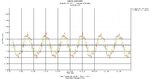
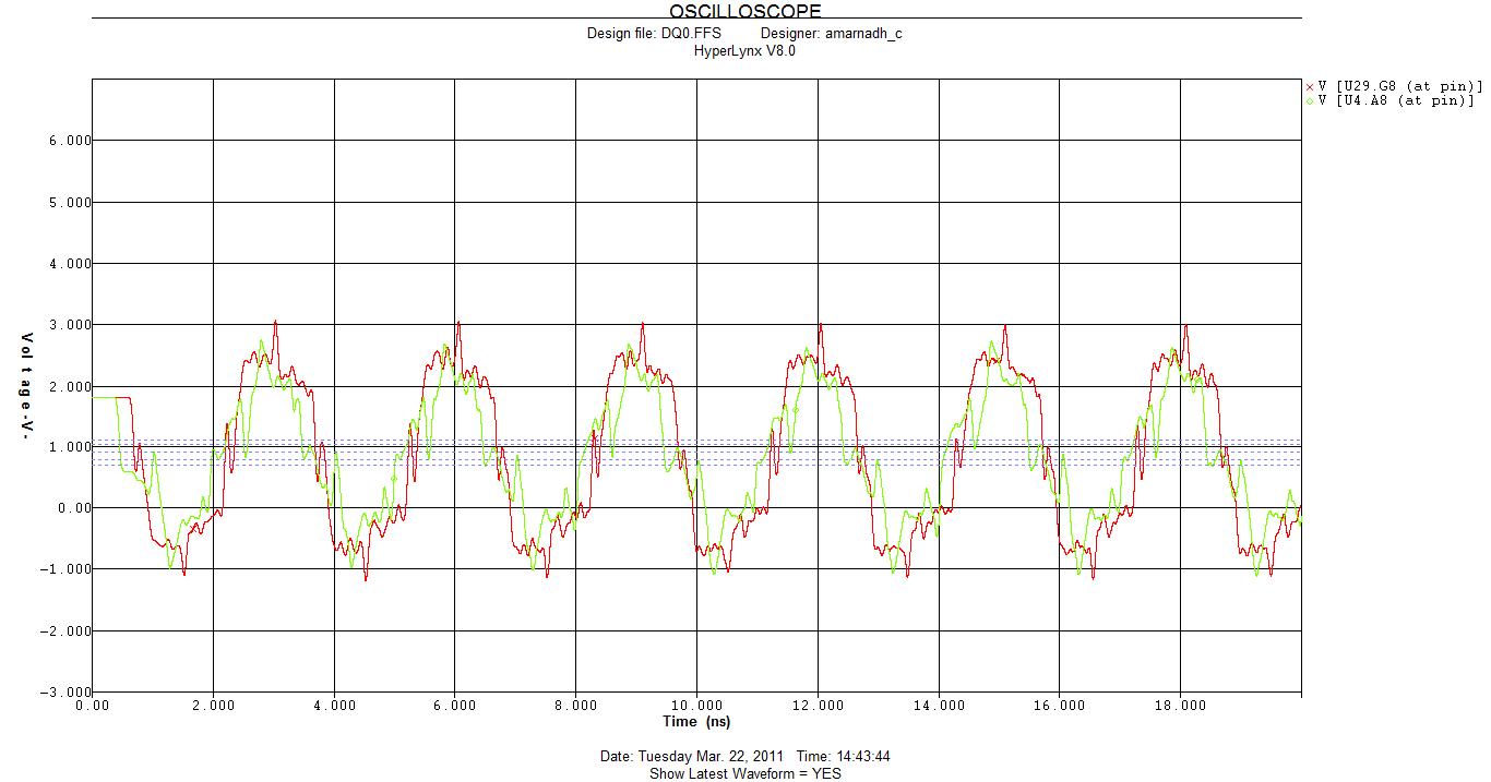
From the waveform it looks like the red waveform is the Receiver waveform. For DDR You can try checking it with by enabling ODT. If you can share the topology that you had followed it would be very clear to help you out.
For Eliminating Ringing try adding up series resistor, but By enabling ODT this should solve the problem, anyways share the topology you followed.
Hi Amarnadh,
From the waveform it looks like the red waveform is the Receiver waveform. For DDR You can try checking it with by enabling ODT. If you can share the topology that you had followed it would be very clear to help you out.
For Eliminating Ringing try adding up series resistor, but By enabling ODT this should solve the problem, anyways share the topology you followed.
Thank you for your support.
Sorry my english is not good.
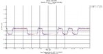
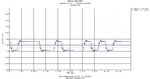
When I enabled ODTs signal voltage level is dropping.I will attach those files.
When I add series resistors, still ringing is there. Iam attaching the stack up details what we are following. please go through and suggest.
is MPC8378 for controller from freescale and NT5TU64M16DG for DDR2 from nanya. I was checked for the equivalent DDR2 from Micron also. still the same results are coming.
Thank you for your support.
Amarnadh.
Hi,
Hey ur welcome, Don bother about English, This is place to support each other.
I need clarification, if DDR speed is 667 Mbps, then u simulate DATA,STROBE and CLOCK at 333MHz is it not? Address will be 333/2MHz. What is the impedance you maintained, I don think am able to view the stack-up details.
You are getting reflections because there is mismatch between driver and receiver. Can you provide your topology as how you connected Driver and Receiver.
Hi,
If it is DDR667Mbps, then you must simulate with the following,
data/data mask nets as 667Mhz,
strobe(dqs), clock = 333Mhz
control nets = 333Mhz
address/commnad = 333Mhz if it is IT clocking scheme or 166 for 2T.
For the simulation you must use models from the micron for the memory chip cause you have mentioned the part no as MT47H128M16. The models of the part will be readily available from the micron website. Check the below link for the model.
**broken link removed**
You don't need to worry about the voltage reduction until it meets the threshold values. let me know if you have doubts in threshold values for logic 1's and 0's.
We can still live with ringing until it wont crosses the overshoot and undershoot values which causes reliability issues, crosstalk and EMI.
Change the address daisy chain routing to the T-Point routing and place the VTT termination at the junction point and make sure the signals from t-junction to all the 4 memory chips are same. You need to run a simulation to find out the maximum trace length from processor to T-junction and from T-junction to the memory chips. It is very simple to do that. This will solve your address/cmd/control issue.
SSTL18 is the standard logic level for the DDR2. Refer the attached JEDEC standard.
The maximum limit for overshoot/undershoot are 2.1 and -0.3V respectively for all the DDR2 signals.
Let me know for more queries.
Thanks
Shiva
Hi,
Wat Sivalingam suggests is a good idea. Your signals are well cleared of the problem.
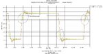
Run the waveform with duty cycle 50% and check it for receiver.
Even though the layer 4 seems signal, it is better to route in inner signal layers both 8 and 10 has reference planes on both sides.
For the non-monotonic edges still if u feel troubled about it, you would have done timing analysis right?
Check the delay with your analysis and I don think it would become a problem.
Hi Everybody...
Recently I have simulated a DDR2 266 MHz/533 Mbps memory interfaced with Power QUICC processor to analysis following Results that affect signal quality at the receiver for SSTL 18 signaling…
Proper selection of termination value (ODT)
Data Valid Window & Timing margins (Eye Width & Eye High)
Timing Budget calculations (read & write cycle)
Slew Rate
Over-shoot & Under Shoot
Cross talk analysis
If you have any doubt related to DDR2 Memory Interfaces I may help you….