Continue to Site

Welcome to EDAboard.com

Welcome to our site! EDAboard.com is an international Electronics Discussion Forum focused on EDA software, circuits, schematics, books, theory, papers, asic, pld, 8051, DSP, Network, RF, Analog Design, PCB, Service Manuals... and a whole lot more! To participate you need to register. Registration is free. Click here to register now.

Question on using CMFB

Status
Not open for further replies.

Ravinder487

Full Member level 3
Joined
Jul 9, 2010
Messages
169
Helped
0
Reputation
0
Reaction score
0
Trophy points
1,296
Location
Bangalore, India
Activity points
2,469
Hi all,
As I understand CMFB is used to fix the output nodes at some fixed voltage even in presence of any mismatches between two wings of differential amplifier.
If this is true while simulating a basic differential amplifier we don't consider any mismatches,so is there any need to include CMFB (at least for simulation sake).
 

I`m not sure if this answers your question - nevertheless:
CMFB is to be applied for fully differential (FD) stages only. For single output stages you apply feedback for gain determination as well as operating point stabilization. For FD applications you must stabilize/optimize both dc output voltages at the same time - independent on gain fixation. Thus, you need a separate feedback scheme for the operating point only. That`s the CMFB branch.
 
@LvW:Is my perception right or wrong?
yeah we need to stabilize,but what will cause voltage unstabilized?(to me it seems like process variations and mismatch)
 

In simple words, you may find it extremely difficult to keep your output transistors in saturation without a cmfb. The best way to learn is to try it out yourself.
 
Hi,
OK, you did it.
But try to answer those following Q:
What is output CM?
Who determine the output CM?
If nobody, you should have it determined.
LEE
 

yeah I tried it and I got gain as expected!!
Oh good! It's your lucky day then ;p
If you look at your output stage, have you ever wondered who controls your output current?

Basically, both the PMOS and NMOS current mirrors are trying to force a current at the output.
Device mismatch, short channel, systematic offset, channel length modulation, just some of the long list of possible causes for a current mismatch.

If you have a low gain, you may be lucky to remain in saturation, or even luckier if both try to force the exact same current.
Otherwise, what you'll see is that one of the mirrors will "win" and push the other into the linear region.

You really need a CMFB in fully differential circuits. It is strictly necessary. Stabilizing the output CM is an hard task in ideal conditions, for the systematic offset, the differences between nmos and pmos characteristics. Thus, a fine tuning of the size of the transistor is required to match the specification on the CMO. However, being Rout high in most cases, just a little error between the currents push low or high your CMO. Besides, a fine tuning of the transistor size is quite a nonsense because of mismatch. However, without a CMFB your fully diff won't work in real cases..with a lot of luck in ideal cases it may work, but this is not the point.
 
Hi all,
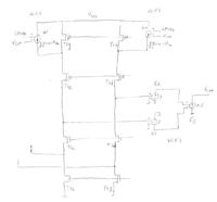
I've found this circuit,on edaboard, for simulating ideal CMFB but I couldn't understand how does this work.
 

The VCM as indicated on your pic should be connected at the CMFB amplifier and not be left on air as the image shows.

The right most sources are nothing else but VCVS to model an ideal CM voltage sensing procedure that is realized with large resistors in practise.Write down the equations from the outputs of the amplifier up to the VCM node on the pic and you will get what you ask by yourself!
 
@Jimito:Yeah I've tried a lot but couldn't get an inch of it!!By the way what is ggain in circuit and what should be its value(shown as 10 in fig) and what is CMref, how can I decide its value!!
 

The principle is simply negative feedback.
Consider the low side as a current source with short channel effects.
If Vcm<CMRef, it means we need more current in the output stage, which is sourced by G1 and G2.
If Vcm>CMRef, it means we need less current in the output stage, which is sunk by G1 and G2.

ggain is the amplifying component of the common mode gain ... the higher the better.
 
@Checkmate:Sorry for asking you again the same question,how do I decide the value of CMRef.Is it Vdd-Vds1-Vds2??
 

Let's say that your amplifier has a common mode output level X mV for the ideal state without the CMFB amplifier (this situation exists only in simulations where you control of the appearance of various mismatches,process variations etc... that could affect this potential) and for this level you reach your specs.Thus,the desired output CM level is XmV consequently Vref=X mV.
 

@Jimito:Can you please post your design methodology(explain with appropriate node voltages) as I couldn't get how to use that circuit.My method seems to be round about and I need to precisely adjust my W/L so as to keep all transistors in saturation.
 

I would suggest that you read some theory first about the basic concepts of the Common Mode Feedback procedure (Gray-Meyer's respective chapter is a good startup point).It has no meaning to show you a schematic of a complete real circuit without you not having a theoritical background.What i am gonna tell you is the following : for an initial approach of the CMFB amplifier you can use a simple model (with 1-pole or no poles for more simplicity) and see how the whole thing works.This simple model of course should be a vcvs as it would be for an op-amp model.
 

Status
Not open for further replies.

Part and Inventory Search

Welcome to EDABoard.com

Sponsor

Back
Top