Continue to Site

Welcome to EDAboard.com

Welcome to our site! EDAboard.com is an international Electronics Discussion Forum focused on EDA software, circuits, schematics, books, theory, papers, asic, pld, 8051, DSP, Network, RF, Analog Design, PCB, Service Manuals... and a whole lot more! To participate you need to register. Registration is free. Click here to register now.

How to increase the output impedance(gain) of an amplifier with current source load?

Status
Not open for further replies.

thomas00

Newbie level 4
Joined
Nov 26, 2010
Messages
6
Helped
1
Reputation
2
Reaction score
1
Trophy points
1,283
Activity points
1,343
I have a question regarding the gain optimization of an amplifier

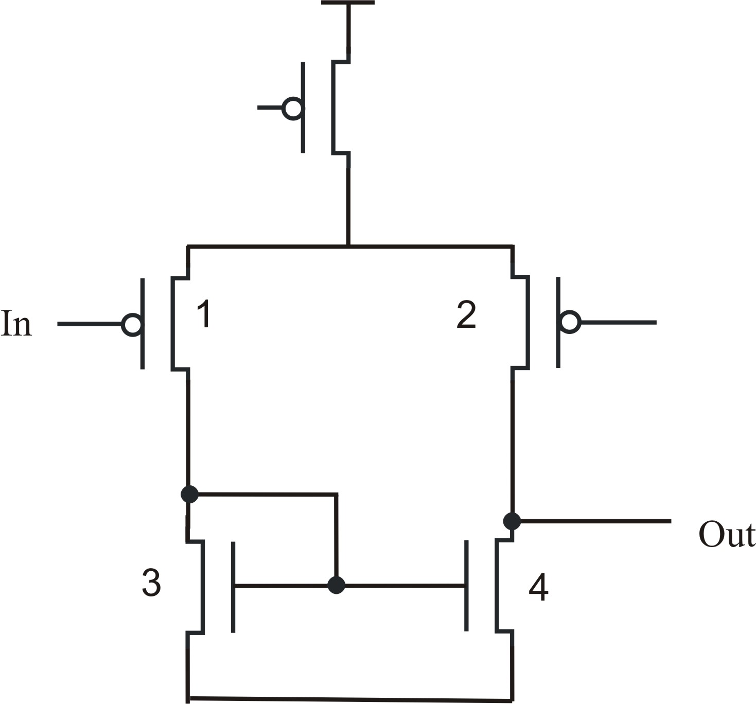
The output gain of a standard differential amplifier can be written as
G=gm1*(r02||r04)
here r02 and r04 are the output impedances of the transistors
Therefore, it is often said that the length of these transistors should be large so that their output impedances are high

But I am thinking which one is dominant in this equation, r02 or r04?
If r04 is dominant, then I only need to increase the length of M4
Otherwise, if r02 is dominant, then it is allowed to use small length for M4 and I only need to use large length for M2.

The same question also applies for a single input amplifier stage, I am not sure if I should optimize the output impedance from the amplification transistor or from the load transistor?


Why do you think, one output impedance would be dominant? Both transistors are operated with same Id, a first guess says, both are equal.
 
If you put source resistors in series with the sources of all fets, the output impedance will increase, but the gain will decline. If you put source resistors on 3 and 4 their output impedance will increase and the gain may go as much as 2x higher.
 
If you put source resistors on 3 and 4 their output impedance will increase and the gain may go as much as 2x higher.

Degenerated current mirrors are an option, but rarely used in CMOS design due to resistor matching problems, I think. A cascode current mirror is the usual methode, if high output resistance is intended.

My previous posted first guess wasn't quite right, I forgot, that the differential pair output resistance is about doubled compared to a current mirror with same transistor parameters and Id.
 
Insert, addtional circuit of current feeback , this is feedback theory trick
 
Have I understood it correctly, that the output impedance r2 of transistor 2 is dominant in the gain rather than the output impedance of r4


Degenerated current mirrors are an option, but rarely used in CMOS design due to resistor matching problems, I think. A cascode current mirror is the usual methode, if high output resistance is intended.

My previous posted first guess wasn't quite right, I forgot, that the differential pair output resistance is about doubled compared to a current mirror with same transistor parameters and Id.
 

Have I understood it correctly, that the output impedance r2 of transistor 2 is dominant in the gain.
I think, without modification of the current mirror, Ro,4 will be about half of Ro,2, in so far, Ro,4 is "dominant" respectively the first candidate for improvement.
 
thanks, I am also quite interested to know why R04 is about half of R02?

Their currents are the same, so the output impedance would be mainly dependent on the length of transistors. So doesn't it depend on different sizing of 2 and 4?


I think, without modification of the current mirror, Ro,4 will be about half of Ro,2, in so far, Ro,4 is "dominant" respectively the first candidate for improvement.
 

You should be able to see operating point Rout or gDS-es
in your simulations, and determine for yourself which FET
is dominating the parallel result.

Note that if either FET gets close to linear region the
result goes in the tank. The smaller the FET width, the
more Vgs at either end and the narrow the non-lousy
region becomes. Running more L does not help if this
is your problem.

Running more W and shorter L will lower Vgs for a given
tail current and make the FETs have more range in
saturation, but you will be more at the mercy of lambda.
You should figure out for yourself whether you are seeing
a saturation-region type of Rout or not, so you know
what's driving your result.
 
As you said in your first post, Rout is ~ro2||ro4. This is the correct one and as you said, in chapter five of razavi's book, you can find that Rout is ro2||ro4 ( equation 5.28 ) .
 

    V

    Points: 2
    Helpful Answer Positive Rating
Cascoding is an option.
I think you don't want one dominates the other in Rout because they are parallel.
 

    V

    Points: 2
    Helpful Answer Positive Rating
Status
Not open for further replies.

Part and Inventory Search

Welcome to EDABoard.com

Sponsor

Back
Top