Continue to Site

Welcome to EDAboard.com

Welcome to our site! EDAboard.com is an international Electronics Discussion Forum focused on EDA software, circuits, schematics, books, theory, papers, asic, pld, 8051, DSP, Network, RF, Analog Design, PCB, Service Manuals... and a whole lot more! To participate you need to register. Registration is free. Click here to register now.

cascode low noise amplifier

Status
Not open for further replies.

bpramee

Newbie level 4
Joined
Aug 10, 2010
Messages
7
Helped
0
Reputation
0
Reaction score
0
Trophy points
1,281
Location
kerala
Activity points
1,335
hi..
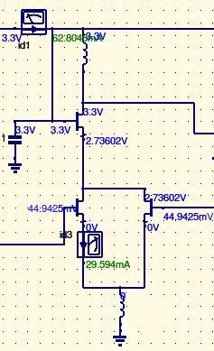
i am trying to design a mesfet low noise amplifier in S band using cascode configuration with Vdd=3.3V . Threshold voltage of mesfet is -0.73. .After calculating the dc bias i got Vgs of upper fet ,M1 (common gate)as 0.57V and that of lower fet,M2 (common source) as 0.04V.
That is M1 is operating in triode region since Vds<Vgs-Vth (3.3<3.3+0.73) and M2 is in saturation.
Is it necessary that M1 also should operate in saturation??current through M2 is 29 mA.Is that current too high??If i try to make M1 in saturation stability will be lost and noisefigure is going beyond limit.. please help
 

I am confused. In a cascode amplifier the drain currents of both transistors should be almost equal.
 

The drain current will be the same for both transistors. Yes, typically you want both transistors in the saturation region. Yes, the cascode cell will be unstable. You will have to stabilize the cascode cell and there are many approaches and techniques for doing this. As for the current being too high, this depends on the transistor size. The current should be specified in terms of a current density per transistor periphery (mA/mm). There is an optimum current density for best noise performance and that value should be supplied from the transistor manufacturer. You should be designing to that current density if noise performance is the main priority. The Vds split between the two transistors will be chosen more for gain performance. That being said, it also has a small effect on noise performance on the first transistor so that will be a trade-off depending on what your specifications are. You choice of Vds on the top device essentially sets the Vds split for each transistor.
 
50_1287554602.jpg

here is my circuit.I have the transconductance parameter beta=0.063(as given in datasheet of mesfet) for my mefet model which is proportional to the width to length ratio.Is it that enough for the transistor dimension? I dont have option for width and length in the QUCS simulator that i am using.Gain,stability and noisefigure are within my design goal using this circuit.But problem is with biasing condition.Upper fet in triode region and lower in saturation.IS it necessary that i should give a negative supply to gate of a mesfet??please help..
 

There are a few things that I am not sure about with your schematic. First, what are the gates of your two lower transistors tied to? Are they just two devices in parallel in which the gates are tied together as well? Second, your top transistor has it's gate tied to the Vdd rail voltage. This device is not really doing anything. It essentially looks like an active switch in the on-state. I think you want to bring the top transistor gate voltage down to give you the desired Vds you want across each device. Then both devices will be in the saturation region and you will be getting better performance. If you are meeting you performance specifications with the circuit you have now, you probably do not need a cascode design. You could remove the top device and go with a single-ended design. That would allow you to reduce the rail voltage, if you can, and conserve power.
 
Status
Not open for further replies.

Similar threads

Part and Inventory Search

Welcome to EDABoard.com

Sponsor

Back
Top